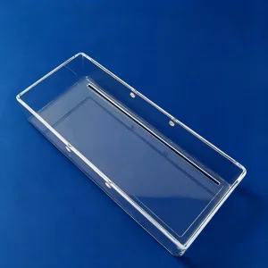
Explore standard and bespoke high-purity quartz furnace components, ring seals, and thermal carriers designed for extreme industrial environments.





Strategic analysis of why Tier-1 technology companies are shifting toward vertically integrated custom quartz manufacturing hubs.
Global semiconductor fabrication lines and high-energy optical integrators demand single-digit trace element contamination (Fe, Al, Ti, Na < 0.1 ppm). International buyers seek raw materials originating directly from high-purity geological clusters like Donghai to mitigate mid-stream tier supply disruptions and geopolitical shortages.
The rapid proliferation of industrial femtosecond lasers and EUV lithography systems requires fused silica windows and mirrors capable of withstanding sustained laser fluency greater than 15 J/cm² at 1064nm. Precision polishing with minimal subsurface damage (SSD) has transitioned from an option to a mandatory qualification criterion.
Modern engineering contracts require full-spectrum documentation, including interferometer wavefront maps (Zygo), spectrophotometer UV-NIR transmission curves, and mass-spectrometry gas integrity reports. Off-the-shelf catalog products are systematically yielding to complete print-to-part engineering workflows.
Deploying specialized synthetic fused silica and natural fused quartz tailored for thermal, structural, and optical excellence.
Low-thermal-expansion quartz diffusion furnace tubes, plasma etch chamber viewports, and multi-wafer slotted quartz boats. Engineered to resist reactive fluorine/chlorine chemistries, prevent thermal drooping up to 1,200 °C, and maintain baseline vacuum integrity inside CVD systems.
Custom beam splitters, UV fused silica windows, and laser debris shields. Featuring deep UV transmission (cutoff < 185nm), transmission homogeneity class 0, and laser damage thresholds designed for fiber-laser cutting heads, chirped pulse amplifiers, and medical optics.
Oversized quartz bell jars and massive crucibles used in single-crystal silicon Czochralski (CZ) pulling. Resistant to high-temperature devitrification caused by prolonged contact with molten silicon baths, ensuring high monocrystalline wafer throughput and yield.
Microfluidic quartz flow cells, spectrophotometer absorption cuvettes, and custom ICP-OES/ICP-MS quartz torches. Pristine baseline transparency across the ultraviolet spectrum allows uncompromised chromatographic peak detection and DNA/RNA quantification.
A multi-generational technology trajectory focusing on ultra-low loss transmission, deterministic computer-controlled optics, and hybrid micro-machining.
Implementation of 5-axis CNC sub-aperture polishing platforms and MRF technology to eliminate mid-spatial frequency errors, routinely securing surface figure errors under λ/20 and surface roughness below 2 Å.
Controlling residual OH-ion concentration from <1 ppm (IR-grade synthetic quartz) for broadband telecom windows up to 3.5 μm, to >1200 ppm for excimer laser optical systems operating without solarization damage down to 193 nm.
Coupling reactive atom plasma (RAP) etching with non-contact chemical planarization, purging micro-fissures and residual shear strain from grinding phases to extend high-power laser optics lifetime by over 300%.
Direct femtosecond laser internal writing (FLICE) inside monolithic fused quartz ingots to produce integrated microfluidic channels, embedded fiber gratings, and lab-on-a-chip optical sensors in single solid-state elements.
Eliminating supply chain uncertainty through international technical compliance, traceable raw material provenance, and certified export packaging.
Every fabricated batch conforms strictly to ISO 9001:2015 quality control systems and SEMI standards (including SEMI E10 and SEMI S2). Dimensional verification is performed on Zeiss 3D coordinate measuring machines (CMM) and laser scanning micrometers with absolute accuracy up to ±0.001 mm.
Our dedicated global logistics support group provides full DDP/FOB/CIF handling with regional warehousing capabilities across the EU, North America, and Southeast Asia. We prepare formal material declaration documents (RoHS, REACH, TSCA, Conflict Minerals) to assure frictionless customs clearance.
Finished components undergo multistage ultrasonic surfactant wash and DI water rinsing (18.2 MΩ·cm) in Class 100/1000 cleanrooms. Items are double vacuum-packed in anti-static, clean-grade PE bags and secured in custom shock-absorbing, export-compliant reinforced wooden suspension enclosures.
Straightforward technical answers regarding raw material selection, manufacturing tolerances, lead times, and thermal management.
Complete product range including oversized processing chambers, optical-grade substrates, high-temperature lamp mounts, and semiconductor cleaning apparatus.