Engineered from natural and synthetic raw quartz reserves, verified through helium mass-spectrometry leak detection, precision laser interferometry, and inductively coupled plasma mass spectrometry (ICP-MS).






From deep ultraviolet (DUV) microlithography to multi-kilowatt laser material processing, optical quartz serves as the foundational substrate where thermodynamic equilibrium and photonic transmission must never degrade.
Lithographic steppers operating at 248 nm (KrF) and 193 nm (ArF) excimer wavelengths require synthetic fused silica of the highest grade. Our materials eliminate compaction, color centers, and solarization under extreme laser fluence.
In 10kW+ CW fiber laser cutting, welding, and directed energy deposition, optical absorption creates destructive thermal lenses. Our ultra-low impurity synthetic silica minimizes bulk absorption below 0.5 ppm/cm at 1064 nm.
Scientific spectroscopy instruments operating across 190 nm to 3500 nm depend on quartz flow channels, bubblers, and cuvettes that offer total chemical inertness, zero fluorescence background, and near-zero bubble/inclusion metrics.
An authoritative analysis of geological raw material reserves, synthetic chemical vapor deposition pathways, and commercial manufacturing bottlenecks facing global fabs and optics integrators.
The global quartz market is experiencing an unprecedented structural divergence. While traditional lighting and commercial-grade tubing market demand has stabilized, the demand for semiconductor wafer process consumables (diffusion furnace tubes, quartz boats, bell jars, and single-wafer etching rings) and optical grade fused silica has outpaced supply by double digits.
Natural quartz sand derived from ultra-pure granitic pegmatite deposits (such as Spruce Pine, North Carolina, and Donghai, Jiangsu) underwent intensive processing to drive transition metals below 10 ppb. However, for extreme ultraviolet and excimer optics, natural feedstocks have given way to synthetic silica produced via flame hydrolysis of high-purity silicon tetrachloride (SiCl4) or octamethylcyclotetrasiloxane (OMCTS), achieving metallic impurity profiles below 0.1 ppb.
Supply Chain Insight: Southeast Quartz integrates strategic raw material stockpiling in Donghai County with precision plasma flame fusing and CNC cold-working, mitigating geopolitical supply disruptions for European and North American OEMs.
Procurement engineers often encounter terminology overlap between "fused quartz" and "fused silica". Scientifically and commercially, the differentiation dictates application performance:
| Property / Metric | Natural Fused Quartz | Synthetic Fused Silica |
|---|---|---|
| Raw Material Source | Purified natural rock quartz (Donghai / Spruce Pine) | Chemical gas synthesis (SiCl4 / OMCTS) |
| Total Metal Impurity | < 15 ppm (Grade dependent) | < 0.1 ppm (< 100 ppb) |
| UV Cut-off Wavelength | ≈ 220 – 260 nm | ≈ 160 – 180 nm (Excimer Grade) |
| Typical Application | Diffusion tubes, wafer boats, crucibles | Photomasks, laser windows, DUV optics |
| Maximum Temp (Continuous) | 1,150 °C – 1,200 °C | 950 °C – 1,050 °C (Higher OH types) |
| Trace Metal Element (ICP-MS) | Aluminium (Al) | Iron (Fe) | Calcium (Ca) | Sodium (Na) | Potassium (K) | Lithium (Li) | Titanium (Ti) | Copper (Cu) |
|---|---|---|---|---|---|---|---|---|
| Optical Fused Silica (ppm) | < 0.05 | < 0.01 | < 0.02 | < 0.01 | < 0.01 | < 0.005 | < 0.01 | < 0.001 |
| Semiconductor Quartzware (ppm) | 8.0 – 14.0 | 0.1 – 0.3 | 0.4 – 0.8 | 0.3 – 0.7 | 0.2 – 0.6 | 0.1 – 0.4 | 1.0 – 1.8 | < 0.05 |
Our fused quartz and synthetic fused silica components are benchmarked across mechanical, optical, thermal, and electrical domains to ensure predictable integration into complex sub-assemblies.
Remarkable thermal shock resilience. Parts can be heated to 1,150 °C and dropped into cold water without micro-cracking.
Unmatched internal transmittance spanning the deep ultraviolet to near infrared spectrum with virtually zero absorption spikes.
Exceptional Young’s modulus and flexural rigidity providing micro-deflection tolerance in pressurized furnace chambers.
Outstanding dielectric constant and low loss tangent across microwave, RF, and megahertz plasma-excitation fields.
Real-world integration data highlighting how Southeast Quartz engineered components resist devitrification, process gases, and mechanical creep in demanding fab and laboratory environments.
In high-aspect-ratio DRAM and 3D-NAND manufacturing, vertical quartz furnace tubes and slotted boats sustain continuous cycles between 400 °C and 1,050 °C under harsh dichlorosilane (DCS) and ammonia atmospheres.
Our heavy-wall, oversized fused quartz tubes prevent sagging or ovalization over 1,500+ thermal cycles, maintaining uniform wafer spacing to ensure tight dopant concentration profiles across 12-inch wafers.
Scientific particle accelerators and inertial confinement fusion research centers require ultra-large diameter optical fused silica window plates (up to 600 mm diameter) exhibiting near-zero wavefront distortion.
Southeast Quartz supplies precision polished synthetic quartz plates exhibiting flatness better than λ/10 (λ=632.8 nm) and parallel tolerances within 3 arc-seconds, withstanding severe synchrotron X-ray radiation flux.
Spaceborne optical earth-observation instruments and stellar trackers operate under wide thermal excursions (-150 °C to +120 °C) and cosmic proton bombardment where traditional glass rapidly turns opaque.
Our radiation-resistant optical silica prism and filter assemblies undergo precision annealing, ensuring zero color-center formation and unwavering transmissivity in low Earth orbit (LEO) mission lifespans exceeding 15 years.
Purchasing mission-critical quartz components requires certified chain-of-custody, chemical testing, cleanroom packaging, and international trade compliance.
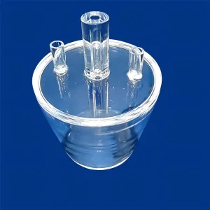
Vacuum-sealed reaction vessels, quartz bubblers, wet oxygen bottles, and multi-port source vessels are 100% helium leak tested prior to dispatch. We guarantee leak rates below 1 × 10⁻⁹ mbar·L/s, eliminating atmospheric contamination risks during CVD and ALD precursor vaporization.
Every melt batch is documented with trace-element ICP-MS spectrometer sheets, stress-birefringence certificates, and 3D CMM inspection protocols. All manufacturing complies with SEMI standards (including SEMI F21-95) and full RoHS 3 / REACH SVHC regulations for frictionless customs clearance globally.
Components undergo ultrasonic 10% hydrofluoric (HF) acid de-staining followed by deionized water cascading to > 18 MΩ·cm resistivity. Parts are double vacuum-bagged in Class 100 cleanrooms and packed in custom CNC-cut foam suspension crates to ensure zero breakage during intercontinental transit.
As semiconductor architectures scale toward 1nm nodes and high-numerical-aperture (High-NA) EUV lithography, our material science engineering roadmap targets the physical limits of silica purity.
Development of rare-earth doped synthetic quartz rings and liners for dry etching tools (CF4/NF3 plasma), extending component in-chamber erosion lifetime by > 250% over standard quartzware.
Commercial scaling of Low Thermal Expansion Material (LTEM) titania-silicate glass substrates, achieving surface microroughness Rq < 0.05 nm for pellicle-free High-NA EUV mask infrastructure.
Direct-write 3D laser-machined fused silica photonic integrated circuits (PICs), enabling room-temperature quantum computing repeaters and deep-space gravitational wave detection optics.
In-depth engineering answers addressing devitrification thresholds, machining allowances, OH absorption bands, and cleanroom handling standards.
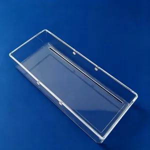
Explore our specialized fused silica rods, 3-port bubblers, high-temperature rings, and wafer cleaning tanks precision-machined to exact customer blueprints.