Direct from Donghai’s premier quartz manufacturing facilities. Certified purity (SiO₂ ≥ 99.995%), thermal shock resilience, and micrometer-level dimensional accuracy.




In modern sub-14nm, 7nm, and advanced sub-3nm node fabrication, the quartz precision ring is far more than a passive hardware spacer—it is an electro-dynamically active plasma consumable.
In high-density plasma dry etch chambers (RIE, ICP, CCP) and chemical vapor deposition (LPCVD, PECVD, ALD), the precision quartz ring—commonly serving as a focus ring, plasma confinement ring, wafer edge clamp ring, or pedestal shield ring—plays a critical role in controlling plasma sheath boundary uniformity, thermal dissipation, and RF coupling integrity. A minor geometric variance exceeding 10 micrometers or an uncontrolled hydroxyl ([OH⁻]) concentration gradient across the ring will warp the equipotential line near the wafer bevel, inducing non-uniform edge etch rates, dielectric breakdown, and devastating wafer yield losses.
Maintains a consistent dielectric constant (ε ≈ 3.78 at 1 MHz) across wide temperature swings, eliminating parasitic RF capacitance and maintaining plasma sheath boundary stability at wafer perimeters.
Specially thermally conditioned to resist CF₄, C₄F₈, SF₆, and NF₃ radical bombardment. Minimizes physical micro-trenching, surface flaking, and airborne particulate shedding under high-energy ion etching.
Manufactured on 5-axis ultrasonic CNC grinding centers. Delivers true positional concentricity ≤0.01mm, parallel flatness ≤0.005mm, and surface roughness down to Ra ≤ 0.05μm (optical super-polish).
How Lianyungang Southeast Quartz leverages deep geographical clustering, vertical integration, and robotic cold machining to deliver tier-1 quality at 30-45% cost savings.
Situated in Donghai County, Jiangsu Province—recognized globally as the crystal and high-purity quartz distribution capital of the Eurasian continent—our factory operates inside an unmatched industrial ecosystem. Over 70% of China's high-purity quartz processing capacity, plasma arc smelting infrastructure, and analytical testing laboratories are concentrated within a 30-kilometer radius.
For international tier-1 semiconductor equipment OEMs (ASML, Lam Research, Applied Materials, Tokyo Electron compatible architectures) and wafer foundries (TSMC, GlobalFoundries, SMIC), this geographical concentration translates directly into:
Concentration in parts per million by weight (ppm / μg/g)
| Element | Standard Grade | Semi-Prime Grade | Synthetic Grade |
|---|---|---|---|
| Aluminum (Al) | 14.0 - 18.0 | 6.0 - 10.0 | < 0.05 |
| Iron (Fe) | 0.15 - 0.30 | < 0.08 | < 0.02 |
| Sodium (Na) | 0.70 - 1.20 | < 0.30 | < 0.01 |
| Potassium (K) | 0.60 - 1.00 | < 0.20 | < 0.01 |
| Total Trace Elements | < 25.0 ppm | < 15.0 ppm | < 0.5 ppm |
The confluence of AI accelerator demand, 3D NAND vertical scaling (>300 layers), and wide bandgap power electronics is reshaping precision quartz ring specifications.
High Aspect Ratio (HAR) contact etch requires ultra-high RF bias power. Quartz rings must resist cryogenic and elevated plasma chemistries without localized arc discharge or thermal micro-cracking.
Silicon Carbide and Gallium Nitride epitaxy operates at extreme thermal regimes (>1,600°C). Precision quartz shield and support rings maintain structural geometry without viscous creep deformation.
Co-packaged optics (CPO) and AI data center interconnects demand optical collimation rings with extreme surface planarity (λ/10) and internal transmission >92% in deep ultraviolet (DUV) wavelengths.
With defects under 10nm destroying advanced logic yields, precision rings now undergo specialized chemical mechanical polishing (CMP) and high-temperature flame annealing to completely eliminate sub-surface damage (SSD).
Tailored geometric configurations engineered for distinct vacuum and thermal chambers across the microelectronics lifecycle.
| Application Scenario | Ring Type & Geometry | Critical Operating Parameters | Technical Failure Mode Prevented |
|---|---|---|---|
| Plasma Etch (RIE/ICP) | Focus Ring, Edge Ring (Stepped, Beveled) | Fluorinated/Chlorinated plasma, 13.56 MHz / 2 MHz dual-frequency bias | Edge roll-off, critical dimension (CD) non-uniformity across 300mm wafer bevel |
| Epitaxy / MOCVD | Susceptor Retaining Ring, Pedestal Shield | Atmospheric to low vacuum, H₂/NH₃ ambient, 1,050°C - 1,200°C | Wafer slip during high-speed rotation, parasitic chemical vapor deposition |
| Diffusion & Oxidation | Tube Seal Flange Ring, Baffle Ring | Wet/Dry O₂, Steam ambient, 1,150°C continuous thermal dwell | Atmospheric contamination leakage, thermal gradient stress fractures |
| Deep UV Lithography | Optical Collimation Reticle Ring | 193nm / 248nm excimer laser illumination, high photon density | Solarization, color-center formation, thermal wavefront distortion |
| Photovoltaic TOPCon/HJT | Tube Furnace Insertion Ring, Boat Collar | POCl₃ diffusion, corrosive gas exhaust, 850°C - 950°C | Phosphorus glass accumulation, wafer contamination and edge chipping |
Rigorous metrology and quality verification ensure zero defect arrival for global buyers across North America, Europe, and Asia-Pacific.
All sealed, flanged, or welded ring assemblies undergo 100% helium leak detection. Leak rates are guaranteed under 1 × 10⁻⁹ mbar·L/s, ensuring absolute ultra-high vacuum (UHV) hermetic integrity.
Residual internal stress induces catastrophic breakage under furnace ramp rates. We utilize multi-point laser polariscopes ensuring optical retardation path difference is strictly ≤ 10 nm/cm after final thermal annealing.
Full dimensional inspection performed via Carl Zeiss Coordinate Measuring Machines (CMM). Every delivery includes a comprehensive dimensional inspection report matching customer GD&T drawings (PDF, DWG, STEP).
To obtain an immediate technical feasibility assessment and firm quote within 24 hours, our engineering department requests the following data:
Authoritative answers provided by our senior quartz materials scientists and fabrication engineers.
Natural fused quartz is made by melting ultra-high-purity natural silica sand (SiO₂ ≥ 99.99%). It exhibits superior thermal creep resistance up to 1,150°C and excellent structural rigidity at lower cost. Synthetic fused silica is synthesized chemically via silicon tetrachloride (SiCl₄), yielding zero bubble content, virtually no metallic impurities (total metals < 0.1 ppm), and superior optical transmittance down into the Deep Ultraviolet (193nm) spectrum, ideal for sub-5nm lithography and extreme excimer laser setups.
Devitrification (crystallization of amorphous SiO₂ into cristobalite) is catalyzed by trace alkali metals (Na, K, Li) and surface fingerprints at temperatures exceeding 1,000°C. We apply high-temperature HF-HNO₃ acid purification baths to strip all surface contamination, followed by thermal vacuum baking and zero-contact cleanroom double-bag packaging. Handled exclusively with lint-free cleanroom gloves, our rings remain crystal-clear without hazing through extended thermal campaigns.
Yes. Leveraging our proprietary plasma-arc centrifugal fusion reactors and large-bed 5-axis ultrasonic CNC milling centers, we routinely fabricate oversized quartz precision rings up to 1,200mm Outer Diameter (OD). These are widely utilized in 450mm semiconductor wafer R&D chambers, generation 8.5/10.5 flat panel display (FPD) wet-etch systems, and large solar polysilicon crystal pullers.
We offer tailored surface conditioning depending on your chamber functional needs: Diamond ground finish (Ra 0.8μm - 1.6μm) for precise mechanical slip prevention; Optical fire-polished or chemo-mechanically polished (CMP) finish (Ra < 0.05μm) for maximum plasma corrosion endurance; or Controlled sandblasted / textured finish (Ra 3.5μm - 6.0μm) on specific faces to enhance CVD film adhesion and prevent flake spallation onto wafers.
Precision quartz components are highly sensitive to shock waves. Every quartz ring is sealed in anti-static PE cleanroom bags, nested inside custom-molded high-density Polyethylene (EPE) shock-absorbing foam nests, placed in heavy-gauge corrugated cartons, and finally secured inside fumigation-free wooden export crates with tilt and impact indicator monitors.
We support both pilot R&D prototyping (MOQ: 1 - 5 pieces) and full-scale fab replacement contracts (batch quantities > 500 pieces/month). Standard production lead times range from 7 to 14 days for standard dimensions, and 15 to 21 days for complex multi-axis CNC contoured rings requiring specialized diamond tooling.
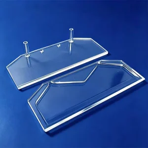
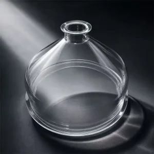
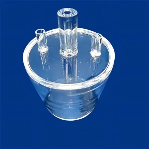
Explore our comprehensive range of companion quartzware: machined plates, high-purity rods, bell jars, and microfluidic detection cells.

Send your 2D/3D CAD drawings (STEP, DWG, PDF) to our Chief Materials Engineer. Receive a full manufacturability review, tolerance analysis, and tiered wholesale pricing within 24 hours.
