Explore our wholesale selection of high-temperature optical plates, vacuum chamber viewports, and custom quartz fabricated parts tested for zero bubble inclusion and trace impurity limits below 5 ppm.





As microelectronics advance beyond 3nm and advanced 3D NAND gate stacking exceeds 200+ layers, the operational thresholds for viewport optics and chamber quartz components have shifted from conventional thermal resistance to ultra-deep UV transmission, zero-defect plasma resistance, and sub-ppb purity control.
Global semiconductor fabs spend millions annually on optical consumables. Premature devitrification, micro-cracking, and plasma erosion result in catastrophic vacuum downtime. Procurement directors prioritize direct OEM relationships that guarantee extended mean time between cleans (MTBC) and mean time between failures (MTBF).
In capacitive coupled plasma (CCP) and inductively coupled plasma (ICP) chambers, fluorine- and chlorine-based etchant radicals bombard window surfaces. Quartz viewports must possess uniform microscopic grain structures to prevent localized spalling, clouding, and silicon particulate shedding onto production wafers.
Modern deposition tools (PECVD, LPCVD, ALD) rely on in-situ multi-wavelength pyrometry and optical emission spectroscopy (OES) through quartz sight glasses. Distortions, thermal lensing, or spectral attenuation in the UV/NIR spectra directly skew temperature measurement algorithms by ±10°C, jeopardizing wafer yield.
Lianyungang Southeast Quartz Co., Ltd. fabricates semiconductor quartz windows utilizing highest-purity synthetic fused silica (JGS1), optical grade fused quartz (JGS2), and infrared optical fused quartz (JGS3). Every optical blank is analyzed for trace element contamination via ICP-MS.
| Material Parameter / Property | Synthetic Fused Silica (JGS1) | Optical Fused Quartz (JGS2) | Infrared Fused Quartz (JGS3) | Semiconductor Standard |
|---|---|---|---|---|
| SiO₂ Purity Grade | ≥ 99.999% (5N) | ≥ 99.99% (4N) | ≥ 99.995% | SEMI C10 / ASTM C-770 |
| Spectral Transmission Band | 185 nm – 2,500 nm (Deep UV) | 220 nm – 2,500 nm (Standard Optical) | 260 nm – 3,500 nm (Full IR) | Spectrophotometer Verified |
| Hydroxyl (OH⁻) Content | 1,200 ppm (UV grade optimized) | 150 – 200 ppm | < 5 ppm (Water-free IR) | FTIR Spectroscopy |
| Coefficient of Thermal Expansion (CTE) | 5.5 × 10⁻⁷ / K (0 – 300 °C) | 5.5 × 10⁻⁷ / K | 5.5 × 10⁻⁷ / K | Zero thermal shock rupture |
| Max Operating Temperature | 1,150 °C Continuous / 1,300 °C Peak | 1,100 °C Continuous / 1,250 °C Peak | 1,150 °C Continuous / 1,280 °C Peak | Softening Point ~1,683 °C |
| Total Trace Metal Content (Fe, Cu, Na, K, Li) | < 1.0 ppm total | < 8.0 ppm total | < 3.0 ppm total | ICP-MS Cleanliness Assayed |
| Surface Figure & Parallelism | λ/10 per inch, < 5 arcsec | λ/4 per inch, < 30 arcsec | λ/4 per inch, < 15 arcsec | Zygo Laser Interferometry |
| Surface Roughness (Ra) | < 0.5 nm (Super-polished) | < 1.0 nm (Standard Optical) | < 0.8 nm | Atomic Force Microscopy |
From extreme-ultraviolet (EUV) source containment to rapid thermal annealing (RTA) optical coupling, custom engineered quartz windows operate as the critical physical barrier between aggressive process vacuums and external metrology systems.
Integrated as top-lid observation ports, laser interferometry end-point detection (EPD) windows, and optical sensor covers. Designed with chamfered O-ring grooves (CF, ISO-KF, ConFlat) and stress-free annealing to withstand cyclic differential pressures of 10⁻⁷ Torr up to atmospheric backfills.
During RTP, spike annealing, and epitaxial silicon growth, quartz windows transmit intense infrared radiation from halogen lamp arrays directly to the wafer substrate. High thermal homogeneity prevents uneven heating zones, safeguarding wafer lattice perfection.
Utilized as entrance viewports, beam splitters, and protective debris shields in DUV (193 nm ArF immersion, 248 nm KrF) and EUV vacuum loadlocks. Exceptional solarization resistance prevents UV-induced color center formation and optical opacity over billions of laser pulses.
Continuous wafer scaling drives radical material advancements in fused silica synthesis, precision plasma-assisted polishing, and structural engineering to meet the exacting criteria of upcoming angstrom-era semiconductor fabrication.
Transitioning from flame-fusion to induction plasma-fused synthetic ingots, driving total transition metal contamination below 0.5 ppm while maintaining bubble-free homogeneity across plates up to 800 mm in diameter.
Deploying deterministic sub-nanometer magnetorheological finishing (MRF) and IBF corrective polishing to achieve surface roughness Ra < 0.2 nm and transmissive wavefront error < λ/20 on complex geometry viewport steps.
Integrating chemical vapor deposited (CVD) yttrium oxide (Y₂O₃) and high-density aluminum fluoride barrier coatings on quartz substrates to achieve a 5x extension of optical window service life in atomic layer etching (ALE).
Embedding high-temperature fiber optic thermal probes and strain sensor arrays directly within laminated quartz sight structures to provide real-time vacuum seal integrity and thermal degradation telemetry.
With massive semiconductor fab construction across the United States, the European Union (European Chips Act), Japan, South Korea, Taiwan, and Mainland China, supply chain agility for custom quartz components has become a geopolitical imperative.
Leading vacuum equipment manufacturers require qualified second-source quartz fabricators to alleviate production bottlenecks. Southeast Quartz maintains dedicated tooling setups and rapid prototyping workflows to transition 2D customer drawings (DWG, DXF) and 3D CAD files (STEP, IGES) into approved initial articles within 7 business days.
Situated in Donghai County, Jiangsu Province—globally acknowledged as the premier fused quartz refining and distribution hub—Southeast Quartz leverages direct upstream access to highest-grade natural rock crystal and purified silica precursors. This geographical cluster ensures continuous material access regardless of international freight disruption.
To eliminate unplanned fab shutdowns, we offer blanket purchase agreements (BPA) with managed safety buffers. Customized quarterly release schedules and export packing compliance prevent transportation damage, guaranteeing vacuum components arrive ready for cleanroom assembly.
Every semiconductor quartz window leaves our facility supported by a comprehensive Certificate of Analysis (CoA), material traceability documentation, and non-destructive inspection records verified against international vacuum standards.
100% helium leak detection on all flanged viewports and sealed components, ensuring an ultra-high vacuum seal integrity with leak rates < 1×10⁻⁹ mbar·L/s.
Precision polarimeter inspection verifies zero residual internal strain birefringence (optical path difference < 5 nm/cm), preventing mechanical shattering during rapid heating.
Glow Discharge Mass Spectrometry (GDMS) detects 64 metallic elements down to ppb trace levels, preventing iron, sodium, and copper contamination of silicon wafers.
Multi-stage ultrasonic acid leaching followed by 18.2 MΩ deionized water cascade rinsing, baked dry, and vacuum-sealed in double anti-static cleanroom pouches.
Key technical insights on selection, tolerances, maintenance, and ordering parameters for fab process engineers and equipment procurement managers.
JGS1 is synthetic fused silica synthesized from SiCl₄; it contains no bubbles or inclusions, has ultra-high deep UV transmission down to 185 nm, and is ideal for lithography and laser metrology. JGS2 is optical-grade fused quartz manufactured from high-purity natural crystal, offering excellent standard optical clarity (220 nm–2,500 nm) for CVD/PVD viewports. JGS3 is vacuum-melted quartz with hydroxyl (OH⁻) content below 5 ppm, preventing water absorption bands in the infrared spectrum (2,600 nm–3,500 nm), essential for optical pyrometers and IR heating lamps.
Devitrification (transformation from amorphous silica to crystalline cristobalite) occurs above 1,150 °C, especially when surface contaminants such as alkali metals (Na, K, Li) or alkaline earths (Ca, Mg) are present. To prevent devitrification, Southeast Quartz executes thorough hydrofluoric acid etching and ultra-pure water rinsing before high-temperature vacuum annealing. Fabs must handle quartzware strictly with talc-free nitrile gloves and avoid fingerprints or grease contact prior to chamber firing.
Yes. Our precision cold-machining facility utilizes multi-axis CNC milling, diamond wheel grinding, and ultrasonic micro-drilling. We routinely machine stepped viewports, circular/racetrack O-ring grooves conforming to MIL-G-5514 / ISO standards, blind mounting holes, edge chamfers, and ground bevels according to exact customer CAD files, maintaining dimensional tolerances within ±0.02 mm.
We deliver optical polishes complying with US Military MIL-PRF-13830B Scratch-Dig specifications: standard 60/40 for general viewports, 40/20 for sensor viewports, and 20/10 or 10/5 for critical laser inspection windows. Transmissive flatness is held up to λ/10 per inch, with surface roughness Ra down to 0.5 nm measured via non-contact optical profilometry.
Viewport thickness is calculated using conservative clamped or unclamped flexural stress formulas incorporating fused quartz's design tensile strength (48 MPa with 10:1 safety factor). Finished assemblies undergo hydro-pneumatic proof pressure testing and helium mass spectrometer leak inspection to confirm zero structural deflection or vacuum bypass under continuous process conditions.
Please share: (1) 2D or 3D technical drawing indicating dimensions, thickness, and tolerances; (2) Required quartz material grade (JGS1 synthetic, JGS2 standard fused quartz, or JGS3 low-OH); (3) Optical clarity specifications (scratch-dig, flatness, parallelism); (4) Chamber operating environment (temperature, process gases, vacuum level); and (5) Prototype vs annual production batch volumes. Quotations are dispatched within 24 hours.
Explore additional factory-direct quartzware including specialized furnace tubes, structural support rings, wafer carrier boats, and plasma-fused components engineered for extreme environments.

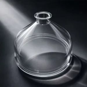

Submit your CAD models, dimensional blueprints, or vacuum flange specifications. Our quartz application engineering team in Donghai reviews manufacturability, optical transmission curves, and thermal tolerances within 24 hours.
