Engineered from synthetic and natural quartz feedstocks for critical thermal stability, high dielectric breakdown, and ultra-low bubble inclusions in cleanroom manufacturing.


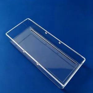


Analyzing raw material geopolitics, sub-5nm fabrication demands, and supply chain vertical integration across East Asia, North America, and Europe.
The global high-purity natural quartz sand supply remains anchored to ultra-pure pegmatite deposits, notably Spruce Pine in North Carolina, USA, alongside emerging refining epicenters in Donghai County, Jiangsu, China. The technical moat lies in ultra-low impurity extraction—specifically eliminating trace alkali metals (Li, Na, K < 0.1 ppm) and heavy transition elements (Fe, Cr, Ni < 0.05 ppm) that trigger premature devitrification into cristobalite at elevated fab temperatures.
In modern 300mm wafer fabs, quartz plates serve primarily as dry etch chamber observation windows, plasma dielectric viewports, showerhead diffusers, and substrate carrier bases. Because halogen plasmas (CF₄, SF₆, Cl₂) erode quartzware through atomic chemical sputtering, fabs execute systematic preventative maintenance cycles, generating continuous recurring replacement demand for certified custom-dimensioned fused silica plates.
The photovoltaic industry's shift from P-type PERC to N-type TOPCon and HJT cells has drastically expanded the use of high-purity quartz plates in low-pressure chemical vapor deposition (LPCVD) and plasma-enhanced chemical vapor deposition (PECVD) tube furnaces. Large-format quartz partition plates and baffles prevent cross-zone thermal interference while maintaining strict particulate isolation, directly governing cell power conversion efficiencies.
From electric arc fusion to synthetic chemical vapor deposition (CVD) and laser cold ablation machining.
| Performance Parameter | Electrically Fused Natural Quartz | Oxy-Hydrogen Flame Fused Quartz | Synthetic Fused Silica (CVD / VAD) |
|---|---|---|---|
| Typical Purity (SiO₂) | 99.99% – 99.995% (4N–4.5N) | 99.995% – 99.998% | > 99.9999% (6N–7N) |
| Hydroxyl (OH⁻) Content | < 5 – 20 ppm (Low-OH / Dry) | 150 – 450 ppm (High-OH / Wet) | Standard: 800–1200 ppm | Dehydrated: < 1 ppm |
| UV Transmission (at 193nm) | < 10% (Significant UV cutoff) | Moderate (30% – 60%) | > 90.5% (Internal transmission > 99%) |
| Bubble Class (DIN ISO 12123) | Class 1 – 2 (Occasional micro-bubbles) | Class 1 | Class 0 (Virtually bubble/inclusion free) |
| Primary Industry Applications | Furnace liners, diffusion baffles, boats | Sight glasses, general labware, lamps | Photomasks, laser optics, wafer viewports |
Operating temperatures inside advanced silicon carbide (SiC) and gallium nitride (GaN) epitaxy reactors exceed 1,200°C. Under continuous exposure to nitrogen and hydrogen atmospheres, pure silica undergoes phase restructuring. By incorporating sub-ppm levels of rare-earth thermal inhibitors during ingot synthesis, modern factories produce quartz plates with a 40% slower devitrification velocity, preventing micro-crack propagation and extending continuous furnace duty cycles.
Traditional mechanical diamond wheel grinding imparts micro-cracks and shear stresses up to 30 microns below the quartz surface, acting as stress concentrators during high-temperature pressure cycles. Leading factories utilize ultra-fast femtosecond laser ablation combined with selective chemical etching (SLE) to cut complex geometries, internal fluidic capillaries, and chamfers without heat-affected zones (HAZ), delivering mechanical fracture strengths exceeding 60 MPa.
For high-end optoelectronic viewports and mask blank substrates, standard double-sided planetary polishing is augmented with Magnetorheological Finishing. By manipulating magnetic fluid carrying cerium oxide nano-abrasives under dynamic computer control, deterministic sub-aperture polishing eliminates high-spatial-frequency errors, achieving wavefront distortions below λ/20 at 632.8 nm and surface microroughness down to 0.15 nm.
Real-world engineering implementations across semiconductor fabs, aerospace avionics, and analytical spectroscopy.
In inductively coupled plasma (ICP) and capacitively coupled plasma (CCP) reactive ion etching chambers, optical quartz plates serve as vacuum viewports and interferometry end-point detection windows. Operating under ultra-high vacuum (< 10⁻⁶ Torr) and intense corrosive fluorine/chlorine discharge, the plates must feature optical flatness < 1 fringe, zero bubble inclusions in the optical path, and specialized sealing chamfers to interface with fluorocarbon O-rings without vacuum micro-leakage.
High-altitude reconnaissance sensors and aerospace optical payloads face acute aerodynamic friction, encountering surface temperatures up to 800°C alongside cryogenic ambient stratospheric air. Custom-dimensioned optical fused silica plates act as pressure-resistant aerodynamic protective shields. Their thermal expansion of 5.5×10⁻⁷/K completely prevents lens warping, preserving infrared and visible image resolution without optical astigmatism.
In i-line (365nm), KrF (248nm), and ArF (193nm) step-and-scan lithography systems, planar synthetic quartz plates are coated with chromium and molybdenum silicide to form circuit photomasks. The quartz substrate must possess extreme spatial refractive index uniformity (Δn < 1×10⁻⁶), zero birefringence (< 2 nm/cm), and negligible thermal drift during gigawatt-level pulsed laser exposure to eliminate optical pattern distortion on silicon wafers.
For single-molecule fluorescence detection, gene sequencing (NGS), and Capillary Electrophoresis, glass autofluorescence ruins diagnostic signal-to-noise ratios. Ultra-pure synthetic quartz plates offer near-zero autofluorescence from 200 nm to 800 nm. CNC micro-milled and chemically polished quartz plates bond with matching cover plates via direct low-temperature plasma bonding, creating bio-inert, non-leaching microchannels.
Comprehensive manufacturing frameworks addressing mounting stress, thermal cycling failure, and specialized coatings.
Prior to manufacturing, engineering drawings undergo coupled thermo-mechanical FEA simulations. Clamping zones are modeled with compliant graphite, fluoroelastomer, or copper-gasket interfaces to calculate peak localized Von Mises stress. Edge chamfering and corner radii are strictly maintained at R ≥ 2.0 mm to remove 95% of perimeter micro-notch stress concentration points.
Every custom machined plate undergoes controlled electric annealing at 1,180°C with an ultra-slow ramp-down rate (0.5°C/min through the transformation zone from 1,120°C to 1,000°C). Residual stress is quantitively validated using Senarmont Polarimeters and high-resolution birefringence cameras, ensuring optical retardation is kept below 5 nm/cm across 100% of the active clear aperture.
To meet complex optoelectronic requirements, custom quartz plates are furnished with high-adhesion PVD coatings inside Class 100 vacuum deposition suites. Available functional coatings include Broadband Anti-Reflective (BBAR) coatings reducing reflection loss to < 0.25% per surface, transparent conductive Indium Tin Oxide (ITO) for electromagnetic shielding, and dielectric hot-mirrors for IR deflection.
Anticipating structural material requirements across sub-2nm Gate-All-Around (GAA) semiconductors, fusion research, and deep-space communications.
Essential guidance for design engineers, procurement directors, and cleanroom process specialists.
Full-scale production capability spanning optical-grade fused silica flats to furnace carriers, bell jars, and CNC machined quartzware.



