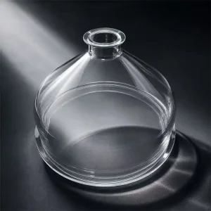
Direct factory fabrication of fused silica substrate plates, furnace core tubes, precision rods, and tailored high-temperature laboratory components.
A comprehensive assessment of synthetic fused silica versus natural quartz plates across semiconductor fabrication, micro-optics, and advanced sensor packaging.
Modern advanced electronics, deep-ultraviolet (DUV) lithography, high-power fiber laser optics, and micro-electromechanical systems (MEMS) demand substrate materials possessing near-zero thermal expansion, phenomenal optical transmission across 190 nm to 3500 nm, and extreme electrical resistivity under high-voltage fields. Custom quartz substrate plates—encompassing both high-purity natural fused quartz (JGS2/JGS3) and synthetic fused silica (JGS1 / CVD-synthesized amorphous SiO₂)—serve as the indispensable physical foundation for next-generation microfabrication.
Globally, the supply chain for quartz substrate plates has undergone profound restructuring. Historically concentrated among niche European and Japanese synthesis houses, escalating demand in silicon wafer diffusion lines, photovoltaic PERC/TOPCon/HJT chemical deposition reactors, and commercial photonics has catalyzed a migration toward vertically integrated, high-efficiency manufacturing clusters. Sourcing executives and lead process engineers must balance pristine optical homogeneity and trace element suppression (specifically eliminating alkali metals such as Lithium, Sodium, and Potassium) against rigid supply chain lead times and cost-volume scaling.
Synthesized via chemical vapor deposition of silicon tetrachloride (SiCl₄) in an oxy-hydrogen flame. Characterized by negligible metallic impurities (< 1 ppm total metals) and no bubble inclusions.
Manufactured by high-temperature electric or oxy-hydrogen gas fusion of premium natural quartz crystal powder. Delivers supreme mechanical integrity and exceptional thermal stability.
Vacuum-fused to strip hydroxyl radicals (OH content < 2-5 ppm), eliminating the 2.73 µm absorption band. Engineered exclusively for infrared thermal imaging and laser cavities.
Unlocking vertical raw-material integration, rapid prototyping, and sub-micron CNC cold processing inside China's primary silica capital.
Proximity to regional plasma-fusion furnaces and high-purity quartz ore processing cuts raw material transit to zero, ensuring immediate raw stock verification and complete batch traceability.
Equipped with ultrasonic CNC milling stations capable of drilling micro-holes down to Ø0.2 mm, step-counterboring, and custom edge chamfering (C-chamfer, R-edge) without micro-crack initiation.
Multi-stage chemical mechanical planarization (CMP) yields extreme surface flatness (< λ/4 per 100mm), Total Thickness Variation (TTV) < 2 µm, and Ra < 0.2 nm for atomic layer deposition (ALD).
All finished substrate plates undergo Class 1,000 / Class 100 cleanroom ultrasonic baths in multi-stage HF / HNO₃ acid chemistry to strip metallic particles, followed by 18.2 MΩ·cm DI water rinse.
In high-volume industrial procurement, the typical bottlenecks faced by European, American, and Japanese OEMs are excessive quotation cycles (weeks) and prolonged machining lead times (8 to 14 weeks) for custom plate geometries. Operating from Lianyungang Southeast Quartz Co., Ltd. in Donghai County breaks this barrier. Combining in-house plasma-fused ingot slicing, high-speed wire saws, precision double-sided lapping machines, and continuous annealing lehrs allows custom substrate prototypes to ship in 5 to 7 working days, with batch orders scaling seamlessly to thousands of pieces per month.
Comparative physical, optical, and thermal metrics across standard natural quartz, high-purity optical fused silica, and synthetic semiconductor grades.
| Physical / Chemical Property | JGS1 (Synthetic Fused Silica) | JGS2 (Optical Fused Quartz) | JGS3 (Infrared Fused Quartz) | Standard Industrial Quartz |
|---|---|---|---|---|
| Primary Application | DUV Optics, Litho Masks, MEMS | Semiconductor Substrates, Viewports | IR Sensors, High-Flux Laser Cavities | Furnace Plates, Thermal Shields |
| SiO₂ Purity Level | ≥ 99.999% (5N) | ≥ 99.995% (4.5N) | ≥ 99.99% (4N) | ≥ 99.9% (3N) |
| Wavelength Transmission Range | 185 nm – 2,500 nm | 220 nm – 2,500 nm | 260 nm – 3,500 nm | 280 nm – 2,200 nm |
| OH Content (Hydroxyl) | 100 – 1200 ppm (Grade Tunable) | 150 – 200 ppm | < 5 ppm (Water-Free) | < 300 ppm |
| Total Metallic Impurities (Al, Fe, Ti, etc.) | < 1.0 ppm total | < 15 ppm total | < 20 ppm total | < 50 ppm total |
| Thermal Expansion (0°C to 300°C) | 5.4 × 10⁻⁷ / °C | 5.5 × 10⁻⁷ / °C | 5.5 × 10⁻⁷ / °C | 5.6 × 10⁻⁷ / °C |
| Softening Point (°C) | 1580°C – 1650°C | 1683°C | 1710°C | 1660°C |
| Dielectric Constant (1 MHz @ 25°C) | 3.75 | 3.78 | 3.78 | 3.80 |
| Surface Roughness (Ra) Capability | < 0.2 nm (CMP Polish) | < 0.5 nm (Super Polish) | < 0.8 nm (Optical Polish) | < 1.5 nm (Fine Ground/Lap) |
| Scratch-Dig Specification | 10-5 / 20-10 MIL-PRF-13830B | 40-20 | 40-20 / 60-40 | 80-50 Commercial |
Fused silica and quartz substrates feature an extraordinarily low thermal expansion coefficient (~5.5 × 10⁻⁷/K), rendering them almost completely immune to severe thermal shock. A precision-cut quartz plate heated to 1100°C can be repeatedly plunged directly into 20°C ambient deionized water without experiencing tensile micro-cracking or structural fragmentation. This property makes them unparalleled for rapid thermal processing (RTP), chemical vapor deposition (CVD), and pulsed high-intensity laser delivery systems.
Devitrification—the polymorphic transformation of metastable amorphous fused silica into crystalline cristobalite—occurs primarily at operating temperatures exceeding 1150°C. Critically, this phase transformation is accelerated exponentially by trace surface contamination, particularly mobile alkali ions (Na⁺, K⁺, Li⁺) and alkaline earth ions (Ca²⁺, Mg²⁺). Lianyungang Southeast Quartz Co., Ltd. counteracts devitrification failure by enforcing rigorous cleanroom HF chemical etching to strip nucleating surface micro-defects, ensuring structural longevity even through repeated 1200°C furnace cycling.
Where standard borosilicate and optical glass fail, custom quartz substrate plates provide absolute chemical, thermal, and dielectric stability.
Synthetic fused silica plates processed to λ/10 wave flatness and super-polished to Ra < 0.2 nm serve as pristine substrates for chromium film deposition in high-precision photolithography mask blanks.
Because fused quartz exhibits an ultra-low dielectric loss tangent (tan δ < 0.0001 at 10 GHz) and high breakdown voltage (25–40 kV/mm), quartz substrate plates are widely adopted for high-frequency RF IC testing and microwave power amplifiers.
With virtually zero autofluorescence under UV and blue light excitation, CNC micro-channeled quartz substrate plates are favored for DNA sequencing flowcells, capillary electrophoresis, and analytical spectroscopy.
Laser damage threshold (LDT) exceeding 15–20 J/cm² at 1064 nm makes synthetic quartz substrates the premier choice for fiber laser cutting protective windows, Brewster windows, and beam splitters.
Large-format quartz plates up to 800 mm × 800 mm act as inert carrier trays and thermal shields in N-type TOPCon and Heterojunction (HJT) cell solar production lines, resisting silane gas decomposition.
Flanged and sealed quartz viewports engineered for high-vacuum, ultra-high-pressure pyrometry, deep-sea research probes, and furnace observation ports handling aggressive corrosive halides.
A technical guideline for process engineers, specifying tolerances, metrology, and helium-leak validation protocols.
To eliminate quotation revisions and ensure first-pass manufacturing yield, procurement and hardware engineering teams should supply the following parameters:
Prior to shipment, every batch of custom quartz substrate plates and associated quartzware produced at Lianyungang Southeast Quartz Co., Ltd. undergoes comprehensive analytical and non-destructive quality verification:
Complete auxiliary quartz components engineered to integrate with substrate processing reactors, diffusion systems, and heavy-duty industrial furnaces.
The evolution from traditional furnace consumables toward atomic-scale flatness, ultra-thin profiles, and AI photonics integration.
Driven by wearable bio-sensing, bendable optoelectronics, and compact RF modules, manufacturers are perfecting continuous CMP grinding of fused silica wafers down to 50–100 µm thickness without structural warping.
As hyperscale AI clusters shift toward optical interconnects (800G / 1.6T transceivers), quartz plates with laser-etched V-grooves act as thermally invariant sub-mounts for arrayed waveguide gratings and laser diodes.
Mainstream semiconductor fabs are transitioning testing, carrier bonding, and wafer-level packaging from 200 mm to 300 mm format. Precision slicing of oversized ingots ensures strict TTV control across the entire 12-inch surface area.
In-depth responses covering material selection, tolerances, chemical cleanability, and thermal reliability.
Send your engineering drawings (PDF, DXF, DWG, or STEP) to our senior technical team for an immediate manufacturability review, material grade consultation, and a transparent factory-direct quotation within 24 hours.