Engineered for uncompromising transmittance fidelity, zero thermal hysteresis, and trace-element purity exceeding 99.999%. Browse our core production lines manufactured in Donghai, Jiangsu.


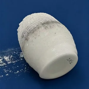


From excimer ultraviolet lithography at 193 nm to infrared pyrometric sensing at 3.5 μm, quartz transmittance is dictated by atomic stoichiometry, hydroxyl (OH⁻) radical content, and crystal structural purity.
Manufactured via silicon tetrachloride (SiCl₄) synthetic chemical vapor deposition (CVD), eliminating transition metal contamination to achieve over 90% internal transmittance at 193 nm and 248 nm. Virtually free from solarization or bubble nucleation under extreme photon flux.
Fused from premium natural crystalline silica through electro-fusion or oxy-hydrogen gas flame processes. Provides excellent transmission from 260 nm to 2,500 nm, making it the dominant industrial benchmark for diffusion process tubes, observation sight glasses, and photolithographic masks.
Utilizes specialized plasma fusion or electric vacuum thermal processing to depress hydroxyl content below 2–5 ppm. Completely eliminates the pronounced 2,730 nm (2.73 μm) OH⁻ absorption band, enabling high-transmittance performance across the Mid-IR range up to 3,500 nm.
| Optical Grade | Material Origin | Spectral Bandwidth | Typical OH⁻ Concentration | Internal Transmittance (T%) | Target Industrial Usage |
|---|---|---|---|---|---|
| JGS1 (Far UV Grade) | Synthetic Vapor Phase (SiCl₄) | 185 nm – 2,500 nm | < 1,200 ppm (Controlled) | > 91.5% @ 193 nm / 248 nm | Excimer Laser Mirrors, Semiconductor Steppers, UV Water Sterilization |
| JGS2 (Standard Optical) | Natural High-Purity Donghai Crystal | 220 nm – 2,500 nm | 150 – 200 ppm | > 92.0% @ 550 nm (Visible) | Furnace Observation Windows, Quartz Flanges, CVD Bell Jars, Solar Tubes |
| JGS3 (Infrared Grade) | Vacuum Plasma-Fused Silica | 260 nm – 3,500 nm | < 3 – 5 ppm (Ultra Low) | > 88.0% @ 2,730 nm | Infrared Pyrometry Sight Glasses, High-Power IR Lamp Envelopes, Aerospace Sensors |
| Opaque / Translucent | Controlled Bubble Micro-Dispersion | Broadband Diffusive | N/A (Structural Scattering) | Diffuse Reflection > 90% | Thermal Heat Shields, Low-Particle Furnace End-Plugs, Flange Thermal Blocks |
Theoretical transmission of pristine fused silica in air is governed by Fresnel surface reflection: $R = \left(\frac{n - 1}{n + 1}\right)^2$. With a refractive index of $n \approx 1.458$ at 589 nm, two bare optical surfaces incur an intrinsic loss of approximately 6.94%, capping theoretical external transmittance at 93.06%. For missions requiring >99% efficiency, Southeast Quartz deploys dual-sided dielectric electron-beam physical vapor deposition (EB-PVD) AR coatings adapted to vacuum bake-outs up to 800 °C.
How semiconductor fabs in Dresden, photovoltaic gigafabs in Southeast Asia, and photonics laboratories in North America configure custom quartz transmittance.
Furnace tubes and carrier boats operating under Low-Pressure Chemical Vapor Deposition (LPCVD) and Rapid Thermal Annealing (RTA) require uncompromised infrared penetration for uniform thermal fields while avoiding wafer slippage up to 1,200 °C.
PV manufacturing centers deploy oversized fused quartz tubes exceeding 450 mm diameter. High transmittance ensures rapid radiative thermal ramp rates, reducing process cycle duration during POCl₃ diffusion and boron doping cycles.
Maritime ballast purification and municipal water sanitization demand thick-walled quartz protective sleeves offering >88% external transmittance at the germicidal 253.7 nm mercury resonant emission band under high hydrostatic pressure.
Micro-channel flow cells and cuvettes require precision flame-polished quartz optical windows. Zero autofluorescence and sub-micron dimensional tolerances enable ultra-trace DNA sequencing and quantitative fluorescence spectrophotometry.
Strategically based in Donghai County, Jiangsu Province—the global hub of crystalline and fused quartz processing. Southeast Quartz operates a vertically integrated production chain from high-purity silica synthesis to certified vacuum-tight delivery.
By positioning our facilities at the epicenter of raw crystal purification, we eliminate raw material bottlenecks. Over 500 metric tons of continuous-drawn tubing, thick-walled ingots, and precision ground blanks are maintained in on-site reserves.
Our infrastructure seamlessly integrates hydrogen-oxygen lathe hot-working with 5-axis CNC ultrasonic cold milling. This prevents micro-crack propagation, mitigates residual stress concentrations, and preserves flawless optical clarity through finished components.
Direct factory manufacturing bypasses distributor markups and reduces iteration friction. Custom prototype quartzware transitions from customer STEP/DWG blueprints to verified cleanroom shipment within 10 to 14 business days.
Every piece of custom quartzware undergoes strict mechanical, spectrophotometric, and vacuum validation protocols to protect high-yield industrial processes.
Calibrated baseline spectrophotometers verify transmittance across 190 nm to 3,200 nm, issuing spectral validation curves with designated batch shipments.
Precision vacuum assemblies, flanged reaction vessels, and bubblers receive individual helium sniffer chamber validation up to 1×10⁻¹⁰ Pa·m³/s sensitivity.
Class 10,000 cleanroom cleaning stations execute multi-stage chemical decontamination, neutralizing surface micro-flakes, metallic dusting, and fingerprints.
Fully compliant with SEMI standards for semiconductor equipment consumables, ASTM C729 for silica density, and RoHS/REACH environmental mandates.
As optical interconnects expand and semiconductor fabrication scales below 2 nanometers, fused silica synthesis must push past physical degradation boundaries.
Synthesizing zero-expansion titania-doped fused silica (ULE) substrates with ppm-level thermal variation coefficients, preventing optical wavefront distortion under EUV radiation.
Replacing manual oxy-hydrogen flame annealing with multi-axis robotic CO₂ laser polishing cells, producing surfaces with surface roughness $Ra < 0.2\text{ nm}$ and zero chemical contamination.
Advancing fluorine-doped and OH-depleted cladding structures for multi-kilowatt industrial fiber lasers, mitigating non-linear Brillouin scattering and thermal lens disruptions.
Engineered for extreme thermal cycling up to 1,250 °C, aggressive corrosive atmospheres, and precision optical beam manipulation. Direct from factory workshop.



In-depth technical answers addressing optical transmission loss, thermal shock thresholds, hydroxyl attenuation bands, and drawing tolerances.
