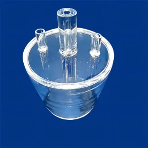
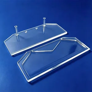
Direct manufacturer supply engineered for microelectronics, high-temperature furnace lines, and extreme vacuum thermal environments.
Although both materials share the identical base chemical formula (SiO₂), their structural arrangement, manufacturing synthesis, and physical behavior diverge substantially across precision industrial applications.
Quartz represents the crystalline state of silicon dioxide characterized by long-range atomic order, typically structured in a trigonal (low quartz) or hexagonal (high quartz) crystal system. Because of its anisotropic molecular alignment, crystalline quartz exhibits distinct piezoelectricity and birefringence, making it essential for radio frequency oscillators, surface acoustic wave devices, and optical waveplates.
However, when exposed to cyclical thermal loads, natural crystalline quartz undergoes phase transformations (such as the α-to-β inversion at 573°C), inducing sudden volumetric expansions that can cause catastrophic mechanical failure in thermal processing equipment.
Fused silica and fused quartz describe the non-crystalline, amorphous (vitreous) modifications of SiO₂. Engineered by high-temperature fusion of ultra-pure natural quartz sands or chemical synthesis (such as CVD flame hydrolysis of silicon tetrachloride), the disordered molecular network results in isotropic physical characteristics.
The vitreous state eliminates crystalline cleavage planes and destructive phase conversions, delivering an extraordinarily low coefficient of thermal expansion (~5.5 × 10⁻⁷ /°C), nearly zero birefringence, superior thermal shock survivability up to 1,250°C, and exceptional optical transmission from the deep ultraviolet through the near-infrared spectrum.
| Performance Characteristic | Natural / Crystalline Quartz | Fused Quartz (Electric / Flame Melted) | Synthetic Fused Silica (Chemical Vapor Synthesis) |
|---|---|---|---|
| Atomic Matrix | Long-range crystalline lattice (Anisotropic) | Short-range vitreous network (Amorphous) | High-homogeneity vitreous network (Amorphous) |
| Typical Purity Level (SiO₂) | 99.5% – 99.9% | ≥ 99.99% (4N) to 99.999% (5N) | ≥ 99.9999% (6N+ Ultra-Purity) |
| Thermal Expansion (CTE) | High & Directional (7.5 to 13.7 × 10⁻⁶/K) | 5.5 × 10⁻⁷ /K (Near-Zero Isotropic) | 5.2 – 5.5 × 10⁻⁷ /K (Near-Zero Isotropic) |
| Continuous Service Temp | Limited (< 573°C Phase Transition) | ~ 1,100°C (Softening at 1,683°C) | ~ 1,150°C (Annealing dependent) |
| Optical Transmission Range | Polarized / Dependent on crystal axis | 260 nm – 2,500 nm (Broad UV-Vis-NIR) | 160 nm – 2,200 nm (Deep DUV Lithography grade) |
| Primary Target Applications | RF filters, timing crystals, optical rotators | Diffusion tubes, semiconductor boats, bell jars | Excimer laser optics, EUV photomasks, space optics |
Strategic analysis of cleanroom consumable supply chains, advanced wafer fabrication nodes, and evolving procurement criteria among Tier-1 industrial buyers.
As semiconductor wafer fabrication transitions toward advanced sub-3nm nodes and complex 3D NAND gate structures, tolerance for metallic contamination (notably Fe, Cu, and alkali elements like Na, Li, K) has dropped below parts-per-billion (ppb) thresholds. Global chipmakers now require synthetic fused silica and plasma-refined quartz furnace furniture to prevent atomic diffusion defects and lattice disruptions during prolonged high-temperature furnace runs.
The photovoltaic sector's pivot toward high-efficiency N-type TOPCon and heterojunction architectures requires oversized diffusion tubes with wall thickness precision under ±0.2 mm and high-purity single-crystal pulling quartz crucibles. Procurement directors demand structural integrity that resists thermal sagging at 1,200°C while resisting devitrification across thousands of continuous manufacturing hours.
Hyperscale data centers and high-density optical transceivers rely heavily on micro-channel flow cells, fused silica windows, and low-hydroxyl (low-OH) capillary waveguides. Enterprise buyers seek suppliers capable of nanometer-level surface roughness (Ra < 0.5 nm) to prevent transmission attenuation and optical scattering in extreme high-bandwidth computing applications.
From initial design simulation to final high-vacuum testing, we engineer application-tailored fused quartz assemblies that solve mission-critical thermal and chemical failure modes.
We engineer end-to-end chamber assemblies featuring oversized fused quartz furnace tubes, high-precision flanges, and automated multi-slot wafer boats. All vacuum-welded assemblies are verified with mass spectrometry leak testing to safeguard zero-defect atmospheres during low-pressure chemical vapor deposition.
For aggressive semiconductor etching and laboratory synthesis involving hydrobromic, hydrochloric, or sulfuric acids at elevated temperatures, our hot-worked 3-port bubblers, source bottles, and continuous reaction columns provide inert, corrosion-free containment that standard borosilicate glassware cannot match.
Utilizing high-purity synthetic fused silica blanks, our cold-machining facility manufactures custom-dimensioned optical flats, irregular windows, and microchannel flow cells with wavefront distortions down to λ/10, supporting high-energy UV lasers, analytical spectrometry, and medical diagnostics.
Minimizing supply chain risk through robust quality systems, material traceability, and dedicated global logistics protocols.
Every batch of raw quartz sand and synthetic precursor undergoes Inductively Coupled Plasma Mass Spectrometry testing to document trace element concentrations, supplying full material test reports (MTR) with every enterprise delivery.
All pressure-bearing tubes, flanged joints, and vacuum reaction chambers undergo calibrated helium mass-spectrometer leak verification before packaging, preventing micro-leak downtime on client manufacturing floors.
Engineered shock-absorbing crates, multi-layer cleanroom vacuum wrapping, and calibrated tip-and-tilt sensors protect fragile oversized quartz tubes during intercontinental ocean and air shipping.
Our senior materials engineering team in Donghai works directly with clients to review CAD/STEP schematics, optimize thermal stress points, select suitable glass grades, and accelerate prototyping cycles.
Anticipating future industry demands through ongoing research in ultra-low hydroxyl synthetic silica, plasma deposition, and additive manufacturing.
Development of proprietary vacuum degassing and electric-fusion processes designed to strip bounded OH radicals from synthetic silica matrices, preventing infrared attenuation and mechanical bubble nucleation at working temperatures exceeding 1,200°C.
Scaling additive micro-plasma deposition for high-purity quartz prototypes, eliminating conventional tooling lead times and enabling complex internal cooling channels within semiconductor showerheads and gas-dispersion nozzles.
Integrating magnetorheological finishing (MRF) and ion-beam milling on CNC machining lines to achieve surface finishes below Ra 0.2 nm, tailored for extreme-ultraviolet (EUV) optical pellicles and photomask substrates.
Clear engineering guidance covering composition, thermal boundaries, maintenance, and ordering details.
Explore our extensive line of durable, factory-direct quartzware ready for custom configurations.