

Ultra-high purity (SiO₂ ≥ 99.998%) quartz thermal and fluid control apparatus engineered for extreme high-temperature and severe chemical environments.




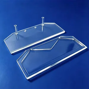
An authoritative analysis of front-end fab material demands, thermal stability thresholds, and chemical inertness under shrinking lithographic nodes.
Modern semiconductor fabrication across advanced nodes (7nm, 5nm, 3nm GAA) has eliminated tolerance for ionic and metallic contaminants. High-purity quartz products with trace elements (Fe, Cu, Ni, Na, K, Li) controlled below parts-per-billion (ppb) levels prevent catastrophic wafer lattice degradation during diffusion, LPCVD, and oxidation processes.
Global semiconductor fab expansions have placed unprecedented stress on certified high-purity quartz processing factories. From natural feedstock refining to CNC ultrasonic cold processing and hydrogen-oxygen thermal fusion, our manufacturing ecosystem provides redundant, scalable capacity to insulate Tier-1 OEMs from raw-material deficits.
Wafer batch processes exceed continuous thermal thresholds of 1150°C with cyclical spikes reaching 1250°C. Fabricated fused quartz demonstrates near-zero thermal expansion (α ≈ 5.5×10⁻⁷/K), eliminating mechanical micro-strains while resisting corrosive halogen and fluorine-based RF plasma etch cleaning cycles.
Standardized and custom quartzware built to endure thermal diffusion, vacuum chemical vapor deposition, and wafer chemical transport.
Oversized fused silica furnace tubes up to 600mm external diameter engineered for vertical and horizontal diffusion stacks. Homogeneous wall thickness profiles prevent thermal runaway, thermal lensing, and stress cracking under rapid heating ramps.
Slot geometries cut using multi-axis CNC machines and micro-sandblasted to avoid wafer slippage and contact lattice scarring. Our quartz boats maintain planar dimensional stability through repeated thermal oxidation cycles without slot bowing.
Monolithic bell jars, quartz rings, and single-piece dry-etch chambers manufactured through precision thermal lathe welding. High resistance to dry etching (CF₄, SF₆, NF₃) ensures longevity and minimizes micro-particulate contamination in chambers.
Every piece of quartzware leaving our manufacturing facility passes traceable physicochemical and structural non-destructive validation.
Inductively Coupled Plasma Mass Spectrometry inspection measures elemental impurities down to sub-ppb thresholds, validating purity for fab front-end applications.
Critical for welded joints, bubblers, and vacuum processing chambers. Our helium leak testing guarantees integrity to vacuum rates lower than 1×10⁻⁹ mbar·l/s.
Full-field optical polarization birefringence testing verifies residual thermal stresses are removed through controlled cleanroom annealing cycles, mitigating thermal shock fracture.
Bridge-type 3D Coordinate Measuring Machines map profiles, circularity, concentricity, and multi-pitch slotted fixtures directly against CAD STEP/DWG drawings.
| Physical / Chemical Parameter | High-Purity Natural Quartz Grade | Synthetic Fused Silica Grade | Standard Industrial Quartz |
|---|---|---|---|
| SiO₂ Purity Level | ≥ 99.998% | ≥ 99.9999% | ≥ 99.90% |
| Hydroxyl (OH⁻) Concentration | < 5 – 30 ppm | < 1 – 1000 ppm (Grade-tailored) | > 50 ppm |
| Transformation Temp / Softening Point | 1075°C / 1683°C | 1050°C / 1600°C | 1020°C / 1580°C |
| Refractive Index (nD 589.3nm) | 1.458 | 1.458 | 1.455 |
| Core Front-End Application | Diffusion Tubes, Wafer Boats, Chambers | Photolithography Masks, Microfluidics | Halogen Heaters, Sight Glasses |
Custom engineering deployed directly to commercial wafer lines, advanced optical fabrication plants, and cleanroom laboratories.
Integrated directly into automated furnace loaders. Our quartzware maintains structural pitch under 1200°C phosphorus/boron thermal diffusion cycles, preventing runout, robotic handling mismatch, and expensive wafer handling lockouts.
Mass production of high-efficiency photovoltaic cells demands oversized quartz furnace tubes (>3000mm length) and specialized multi-wafer carriers to sustain large-scale thermal POCl₃ deposition with reduced replacement turnaround costs.
Microchannel analytical flow cells manufactured using laser direct micromachining and optical contact bonding. Yields optical interfaces transparent from 190nm DUV up to 2500nm Near-IR, free from cement fluorescence degradation.
Strategic manufacturing initiatives keeping pace with next-generation high-NA EUV lithography and 3D heterogeneous integration.
Eliminating microcracking and subsurface damage during mechanical grinding of fused silica via real-time multi-axis ultrasonic resonant cutting tools, increasing thermal crack thresholds by 40%.
Transitioning beyond flame fusion to synthetic PCVD methods, delivering hydroxyl-free (OH < 0.1 ppm) and heavy-metal-free ingots configured for 2nm/sub-2nm logic processing.
Magnetorheological finishing (MRF) and advanced chemical mechanical planarization (CMP) generating surface roughness (Ra) lower than 0.3nm for optics and wafer dry-etch shields.
Next-generation yttrium and aluminum oxide doping of high-purity quartz surfaces to withstand aggressive fluorine-based and halogen plasma etching without particle shedding.
Direct technical answers addressing procurement specifications, mechanical tolerances, and maintenance longevity.
Specialty furnace tubes, carriers, insulation rings, and machined quartz instruments engineered for commercial wafer processing and analytical installations.


