Engineered Quartzware for Semiconductor Thermal Oxidation, Diffusion, LPCVD, and High-Efficiency Photovoltaic Wafers. Factory-Direct Precision from Donghai, China.
Precision thermal-process consumables manufactured from optical-grade fused silica with trace impurity control down to parts-per-billion levels.






An authoritative engineering review of thermal deformation kinetics, devitrification mitigation, and high-density wafer carrier architectures.
In high-temperature horizontal and vertical diffusion furnaces operating between 1,000°C and 1,280°C, fused silica wafer boats are subjected to relentless thermal stresses. Fused silica, an amorphous form of silicon dioxide ($SiO_2$), possesses a near-zero thermal expansion coefficient ($5.5 \times 10^{-7}/K$), affording unmatched resistance to thermal shock. However, when exposed to operating temperatures above 1,150°C over extended cycles, amorphous silica undergoes a phase transformation into crystalline cristobalite—a phenomenon known as devitrification.
Devitrification is catastrophic for semiconductor foundries; it alters mechanical volume, promotes micro-cracking, and sheds silica particles that contaminate active device regions. As an engineering-driven supplier, Southeast Quartz leverages synthetic plasma-fused quartz ingots and low-hydroxyl ($OH < 5\text{ ppm}$) raw materials to dramatically retard phase transition kinetics. Our boats preserve structural geometry, resisting sagging under continuous 200mm and 300mm wafer load profiles.
From classic ladder slotted boats to monolithic CNC wire-sawn cassettes, carrier architecture directly dictates thermal gas dynamics and process uniformity.
Global semiconductor fabrication and photovoltaic cell manufacturing are undergoing generational paradigm shifts. In photovoltaic solar manufacturing, the mass transition from P-type PERC to N-type TOPCon (Tunnel Oxide Passivated Contact) and Heterojunction (HJT) cells requires thermal boron diffusion stages reaching upward of 1,200°C. TOPCon wafer thickness has reduced below $130\,\mu m$, making wafers extremely prone to warpage if the quartz boat's slot pitch or thermal conductivity fluctuates across its rails.
Simultaneously, the surge in Silicon Carbide (SiC) and Gallium Nitride (GaN) wide-bandgap power semiconductor manufacturing introduces aggressive halide gases and elevated annealing thermal ramps. Fused silica boats engineered by Southeast Quartz withstand rigorous hot chemical atmospheres, ensuring high-throughput fab operations without wafer sticking, micro-scratching, or interstitial metal atom migration.
To safeguard gate oxide integrity and minority carrier lifetime in silicon and compound wafers, chemical purity is maintained above $99.998\%$:
Located at Qinghu Industrial Park in Donghai County—the epicenter of the Eurasian quartz raw materials trade—Southeast Quartz secures unmatched direct access to high-purity crystalline quartz sands and continuous electric-fused ingots, guaranteeing continuous supply chain elasticity.
We blend automated 5-axis CNC diamond grinding, multi-wire slotting, and ultra-high-temperature oxyhydrogen cleanroom flame welding. This hybrid manufacturing approach delivers zero-stress structural weld seams and sub-millimeter positional repeatability across all wafer carriers.
Before final dispatch, each fused silica boat and companion furnace tube undergoes rigorous coordinate measuring machine (CMM) verification, helium mass spectrometry leak inspection, and laser interferometry to ensure dimensional stability and bubble-free optical clarity.
Direct comparative reference parameters for semiconductor process engineers, fab equipment managers, and strategic sourcing directors.
| Critical Parameter | Semiconductor Grade (Standard) | Advanced Fab Grade (Synthetic/Low-OH) | Photovoltaic TOPCon High-Throughput |
|---|---|---|---|
| Base Material Purity ($SiO_2$) | ≥ 99.99% | ≥ 99.998% - 99.999% | ≥ 99.99% |
| Hydroxyl ($OH^-$) Content | < 30 ppm | < 5 ppm (High Viscosity Grade) | < 40 ppm |
| Maximum Working Temp (Continuous) | 1,100 °C | 1,180 °C - 1,250 °C | 1,150 °C |
| Thermal Expansion Coeff ($20-1000^\circ\text{C}$) | $5.5 \times 10^{-7} / \text{K}$ | $5.4 \times 10^{-7} / \text{K}$ | $5.5 \times 10^{-7} / \text{K}$ |
| Wafer Sizes Supported | 100mm, 150mm, 200mm (4", 6", 8") | 200mm, 300mm (8", 12") + Custom SiC 6" | M10 (182mm), G12 (210mm) Wafers |
| Slot Tolerances (Pitch / Width) | ± 0.05 mm / ± 0.03 mm | ± 0.02 mm / ± 0.015 mm | ± 0.04 mm / ± 0.03 mm |
| Surface Finish & Weld Zone Treatment | Flame Polished / Stress Relieved | Optical Precision Flame Annealed | Mechanically Chamfered & Annealed |
| Devitrification Inception Time (@1200°C) | > 80 Hours | > 250 Hours (Continuous) | > 100 Hours |
Engineered fused silica boats deployed in precision fab modules, solar cleanrooms, and advanced research facilities globally.
Used in wet and dry oxygen oxidation furnaces at 900°C–1150°C. Zero metal outgassing from fused silica boats ensures zero oxide interface charge defects ($Q_{it}$) and pristine breakdown voltage distributions across entire wafer batches.
Low-pressure chemical vapor deposition involves aggressive silane ($SiH_4$) and ammonia ($NH_3$) gases at vacuum levels. Our precision slotted boats promote uninterrupted gas flow between wafers while resisting thermal coefficient mismatches.
Optimized for high-volume 182mm and 210mm solar wafer loading in horizontal diffusion tubes. Robust rail geometries withstand high thermal cycle frequency, minimizing downtime during automated boat loading and unloading maneuvers.
When wafers transition from ambient to 1,100°C within seconds under halogen lamp arrays, our low thermal-expansion fused silica pins and carrier boats prevent thermal shock breakage and localized shadow cooling.
Engineered specifically for wide-bandgap compound semiconductor fabrication. Features custom cut-out slots accommodating thick, dense substrates, ensuring complete chemical and structural stability under extreme corrosive thermal atmospheres.
Fused silica boats serve as both hot diffusion carriers and transfer racks in acid etching baths ($HF, HCl, H_2SO_4$). They exhibit absolute chemical inertness, with zero leaching into high-purity chemical baths.
In-depth guidance covering design parameters, devitrification thresholds, cleanroom handling, and custom fabrication timelines.
Wholesale fused quartz equipment and custom components engineered to customer drawings and international semiconductor fab benchmarks.

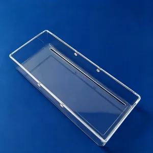

Our quartz engineering specialists review CAD drawings, slot configurations, and equipment parameters within 24 hours. Benefit from Donghai's direct supply chain resilience and competitive volume pricing.
