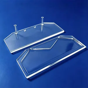
Explore standardized and custom-machined fused quartz assemblies engineered in Donghai County, China. Verified for extreme thermal cycling up to 1,250°C and trace-element purity exceeding 99.99% SiO₂.




Strategic market analysis of microstructural silicon dioxide refinement, opacity mechanics, and next-generation wafer fab thermal insulation architectures.
Historically, fused quartz has served as an indispensable material across semiconductor front-end manufacturing, photovoltaic wafer processing, advanced chemical synthesis, and precision optical instrumentation. However, transitioning device nodes—specifically sub-3nm lithography processes, vertical 3D NAND stack counts surpassing 200 layers, and the mass adoption of TOPCon and Heterojunction (HJT) N-type solar cells—have imposed mechanical, optical, and thermal requirements that standard silica materials cannot satisfy. Polished white quartz components, prized for their superior thermal insulation, high infrared diffuse reflectance, and negligible structural devitrification under cycling conditions, have become vital process enablers.
Polished white quartz achieves its characteristic milky-white opacity through a finely controlled dispersion of microscopic gas bubbles hermetically sealed within an amorphous silicon dioxide matrix. Unlike conventional clear quartz, which transmits infrared radiation directly through its bulk, polished white quartz scatters and reflects infrared wavelengths above 1.5 µm. This optical property creates an exceptional thermal barrier that shields process chambers, flange seals, and heating elements. By polishing these surfaces via flame finishing or micro-grit CNC diamond lapping, factories eliminate micro-cracks, prevent particle entrapment, reduce contamination from alkaline atmospheric moisture, and significantly extend consumable longevity in high-temperature diffusion and oxidation furnaces.
Leading semiconductor fabrication facilities have tightened trace alkali element limits (Li, Na, K) to sub-ppb (parts per billion) thresholds. Transition metal contamination (Fe, Cu, Ni, Cr) must be rigorously suppressed to avoid wafer gate dielectric degradation. Modern quartz factories deploy automated acid-purification lines and plasma-fusion chambers to guarantee raw chemical purity reaching ≥99.999% SiO₂.
The global photovoltaic pivot to large-format M10 (182mm) and G12 (210mm) silicon wafers requires quartz furnace tubes with inner diameters exceeding 350mm to 550mm, combined with lengths up to 3,500mm. Producing dimensionally stable, sag-resistant oversized tubes necessitates refined continuous drawing methods, specialized lathe annealing, and optimized wall-thickness profiles.
Traditional hand-torched glasswork is rapidly modernizing into a hybrid manufacturing paradigm. High-speed 5-axis ultrasonic CNC grinding centers execute tight mechanical slotting (±0.02mm), which is followed by precision robotic flame polishing to remove subsurface micro-cracks and restore maximum mechanical flexural strength without distorting geometric clearances.
Deconstructing the strict engineering, metrological, and material criteria demanded by tier-1 original equipment manufacturers (OEMs) and process fabs.
For global procurement directors, quality assurance managers, and equipment maintenance engineers, sourcing wholesale polished white quartz components involves deep cross-functional vetting. Quartz consumables represent critical single points of failure in semiconductor and industrial furnace hot zones. A premature component fracture, flange leak, or outgassing burst during high-temperature Low-Pressure Chemical Vapor Deposition (LPCVD) or Plasma-Enhanced CVD (PECVD) can ruin a production batch valued in the hundreds of thousands of dollars, while causing days of tool downtime.
Consequently, tier-1 procurement workflows require verified material certifications, transparent lot traceability back to raw mineral sand or plasma-fused ingot ingots, and definitive proof of pre-shipment helium mass-spectrometer leak audits. Below are the primary evaluation criteria utilized by international engineering procurement organizations:
Buyers enforce comprehensive Inductively Coupled Plasma Mass Spectrometry (ICP-MS) inspection reports. Critical threshold elements including Boron (B), Phosphorus (P), Iron (Fe), Copper (Cu), and Sodium (Na) must strictly adhere to SEMI standards to eliminate cross-contamination into sensitive substrate silicon lattices.
Thermal devitrification occurs when amorphous vitreous silica transforms into crystalline cristobalite at temperatures between 1,000°C and 1,200°C, causing surface hazing, micro-cracking, and structural failure. Procurement requires low Hydroxyl (OH⁻) content (typically <20 ppm to 30 ppm) to ensure elevated viscosity and retard thermal deformation.
For oversized quartz furnace tubes, end-cut perpendicularity, circularity/ovality (<0.5% of outer diameter), and wall thickness uniformity are non-negotiable. Wafer transfer robotics require slot pitches on quartz boats to maintain positional tolerances within ±0.03mm across the operational lifespan of the boat.
While direct factory-gate pricing remains a dominant driver, procurement teams prioritize component lifecycle longevity. High-grade polished white quartz collars, rings, and opaque thermal shields reduce heat loss by 25-40%, directly lowering electric kiln power draw while extending maintenance intervals.
| Property / Parameter | Test Standard / Method | Clear Fused Quartz (Standard) | Polished White / Opaque Quartz | Operational Significance |
|---|---|---|---|---|
| SiO₂ Purity Grade | ICP-MS / Spectral Emission | ≥ 99.99% – 99.999% | ≥ 99.98% – 99.995% | Prevents ionic wafer contamination |
| Bulk Density (g/cm³) | Archimedes Immersion | 2.20 ± 0.01 | 2.05 – 2.18 (Micro-cellular) | Lower mass, higher thermal resistance |
| Infrared Transmittance (1.5–4.5 µm) | FTIR Spectrometry | > 85% (Direct passing) | < 8% (High diffuse scattering) | Prevents furnace thermal radiation leakage |
| Softening Point (°C) | ASTM C-338 Thermal Dilatometry | ≈ 1,683°C | ≈ 1,670°C – 1,685°C | Resists sagging at 1,150°C continuous |
| Hydroxyl (OH⁻) Content | Infrared Absorption | < 5 to 30 ppm (Dry grade) | < 20 to 45 ppm | Determines high-temp mechanical viscosity |
| Surface Finish (Ra) | Contact Stylus Profilometry | 0.01 µm (Optical polish) | 0.2 – 0.8 µm (Flame / Diamond lapped) | Prevents particle accumulation & cracks |
Targeted thermal-isolation, corrosion-resistant, and high-vacuum engineering packages designed to resolve demanding industrial challenges.
In silicon wafer fabrication, thermal diffusion tubes operate continuously between 900°C and 1,150°C under aggressive precursor chemistries such as POCl₃, BBr₃, and SiH₂Cl₂. Our integrated solution pairs high-purity clear fused quartz furnace tubes with precision-machined polished white quartz heat shields and baffles. This hybrid configuration keeps the stainless-steel end-flanges safely cooled below 150°C while sustaining an ultra-flat thermal profile (±0.5°C) across the central hot zone.
The industrial scale-up of N-type solar cells involves heavy boron diffusion and plasma-assisted atomic layer deposition. Standard clear quartz carriers suffer premature structural warpage and devitrification induced by frequent loading cycles. We deploy reinforced opaque-to-clear welded quartz boats and thick-walled bell jars engineered with optimized CTE transitions, delivering up to 35% longer cycle lives and suppressing micro-particulate flaking.
In online spectroscopy, environmental monitoring, and high-purity chemical reagent manufacturing, hot mineral acids (except hydrofluoric and phosphoric above 300°C) attack metals and borosilicate glass. Our microchannel flow cells and custom quartz distillation reactors combine precision CNC micro-drilling with optical-grade window fusing, providing complete chemical inertness and maximum UV-Vis spectral transparency down to 190nm.
International quality frameworks, environmental protocols, cleanroom packaging, and supply chain continuity standards.
Procuring engineered quartz components from China requires more than manufacturing capability; it demands verifiable compliance with global trade, environmental, and engineering standards. Southeast Quartz operates an ISO 9001:2015 certified quality management system alongside an ISO 14001:2015 environmental framework. Our engineering workflows translate international technical drawings (ANSI, DIN, JIS) into precise G-code CAM programs with zero misinterpretation of GD&T (Geometric Dimensioning and Tolerancing) parameters.
All raw fused quartz sands, ingots, and chemical purification agents are thoroughly analyzed by accredited third-party laboratories (SGS). Products maintain zero hazardous substance content, fully conforming to EU Directives 2011/65/EU (RoHS) and EC 1907/2006 (REACH) for SVHC (Substances of Very High Concern).
Semiconductor-grade quartz furnace tubes, wafer boats, and bell jars comply with SEMI standards regarding dimensional envelopes, surface roughness (Ra), particle cleanliness, and ionic purity. Material test reports (MTR) are indexed and furnished with every production release.
After final flame polishing or CNC machining, components undergo multi-stage ultrasonic deionized water acid pickling (HF/HNO₃ balance). Parts are dried in a cleanroom environment, followed by double vacuum-sealed polyethylene barrier packaging with desiccants to prevent transit contamination.
Large-diameter quartz tubes and delicate multi-slot boats require specialized shock-absorbent packaging. We employ custom CNC-milled high-density EPE foam cradles enclosed within reinforced, fumigated plywood crates equipped with irreversible 3D shockwatch and tilt sensors to ensure zero shipping loss.
Architectural milestones guiding our investments in synthetic silica deposition, laser cold-machining, and closed-loop quartz circularity.
As semiconductor fabrication migrates toward Gate-All-Around (GAA) nanosheets and advanced 3D packaging, the limits of naturally sourced quartz crystal sand are being reached. Our multi-year engineering roadmap aligns capital expenditure and metallurgical research with the projected performance requirements of global foundries and research consortia.
Commercial deployment of ultra-high-density plasma-assisted sintering for polished white quartz rings and thermal blocks. Reduces micro-pore diameter below 2.0 µm, yielding superior mechanical density and a 40% reduction in thermal conductivity at 1,100°C.
Integration of ultra-short pulse picosecond cold laser ablation units to replace diamond mechanical cutting tools. Achieves microchannel features down to 20 µm with zero heat-affected zones, zero micro-cracks, and pristine surface edge integrity.
Scaling Chemical Vapor Deposition (CVD) of synthetic SiCl₄ precursors to fabricate hybrid dual-layer quartz tubes: an ultra-pure synthetic inner boundary for zero substrate contamination, coupled with an economical natural quartz structural core.
Implementation of an automated optical and chemical recycling circuit capable of recovering spent semiconductor quartz consumables, removing surface contamination layers, and re-melting clean quartz cullet into solar-grade feedstocks.
Comprehensive engineering insights compiled by our materials scientists and export application specialists.
Explore additional engineered quartzware configurations manufactured to custom mechanical drawings. Supported by full helium testing and CNC cold-machining precision.