Direct-from-factory high purity fused silica rods, processing tubes, and wafer handling apparatus rigorously inspected via helium mass spectrometry and spectral trace element analysis.



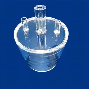

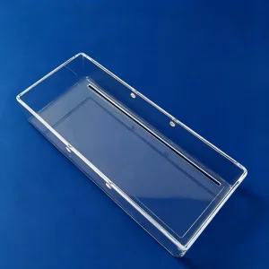

Total metallic impurity levels strictly limited to <15 ppm, with premium synthetic grades hitting <1 ppm.
Extreme thermal creep endurance with continuous 1,150°C loading in LPCVD and fast thermal annealing.
Sub-millimeter laser verification, centerless grinding, and optical-grade flame-polished finishes.
Proprietary flame-fusing tooling, plasma torches, and automated vacuum annealing fixtures.
For procurement leads, wafer fab facilities directors, and plasma etch tooling engineers, specifying quartz rods extends far beyond dimensional diameter. Material behavior at extreme temperatures dictates process stability and wafer yield.
Alkali metals (Na, K, Li) serve as rapid interstitial diffusers within single-crystal silicon, causing gate-dielectric breakdown and flatband voltage shifts. Transition metals (Fe, Cu, Ni) induce deep-level recombination centers.
Hydroxyl groups directly alter the internal network connectivity of amorphous vitreous silica (Si-O-Si bonds). Elevated OH- radicals significantly lower the viscosity, strain point, and softening threshold under elevated furnace runs.
Internal bubble classes, micro-cracks, and particulate inclusion density govern fracture mechanics and particulate shedding inside high-vacuum dry etch chambers (RIE/ICP) under continuous fluorine/chlorine chemistries.
| Quartz Grade Category | SiO₂ Purity (%) | OH⁻ Content (ppm) | Softening Point (°C) | Coefficient of Thermal Expansion (CTE) | Primary Semiconductor Application |
|---|---|---|---|---|---|
| Natural Fused Quartz (Standard) | ≥ 99.99% | 120 – 180 | 1,680°C | 5.5 × 10⁻⁷ / K | Atmospheric Furnaces & Lab Ware |
| High Purity Dehydroxylated Fused Rod | ≥ 99.995% | < 15 | 1,710°C | 5.4 × 10⁻⁷ / K | LPCVD, Oxidation, Wafer Boats |
| Plasma-Fused High Purity Silica | ≥ 99.999% | < 5 | 1,725°C | 5.2 × 10⁻⁷ / K | Advanced 300mm Dry Etch Consumables |
| Synthetic Fused Silica (CVD-Derived) | ≥ 99.9999% | < 10 (Synthetic Dry) | 1,600 – 1,730°C | 5.1 × 10⁻⁷ / K | Photolithography, Sub-5nm Process Chambers |
As semiconductor fabrication transitions to gate-all-around (GAA) nanosheet architectures and 3D NAND configurations exceeding 300 layers, mechanical and chemical demands on quartz rods intensify exponentially.
Devitrification (transition of amorphous vitreous silica into crystalline cristobalite) occurs rapidly above 1,150°C in the presence of surface alkali ions. This crystal transformation induces a 15% volume shrinkage during cooling, causing catastrophic brittle micro-cracking.
Southeast Quartz utilizes multi-stage ultra-pure acid leaching (HF/HNO₃ balance) combined with specialized flame polishing to remove surface micro-pores and hydroxyl nucleation nodes, extending furnace batch campaigns by up to 40%.
In capacitive coupled plasma (CCP) and inductively coupled plasma (ICP) etch environments containing CF₄, NF₃, and SF₆ chemistries, high-velocity ion bombardment attacks Si-O bonds, causing particle shedding onto patterned 12-inch wafers.
Our engineered high-density plasma-fused quartz rods feature minimized structural strain and uniform stoichiometric Si:O ratios, lowering physical sputtering rates and preventing premature replacement cycles in critical wafer-clamping assemblies.
Long vertical furnace rods supporting large mass 300mm silicon boats frequently suffer from gravitational sag at high temperatures. This deformation causes wafer misalignment during automated robotic transfer.
By executing controlled electric fusion and vacuum furnace thermal relaxation at our Donghai manufacturing hub, our rods exhibit superior high-temperature viscosity (>10¹³ dPa·s at 1,180°C), eliminating dimensional warping over multi-week runs.
How material science, advanced synthesis, and atomic-level inspection protocols are evolving to satisfy sub-2nm fabrication nodes and green semiconductor fab mandates.
Transitioning from natural quartz ore to chemical synthetic silicon tetrachloride (SiCl₄) vapor axial deposition. Synthetic rods achieve zero bubble content and total heavy metal levels below 1 part-per-billion (ppb).
Developing yttrium oxide (Y₂O₃) and aluminum oxide (Al₂O₃) nanostructured barrier coatings on quartz rod substrates to resist high-density radical etch erosion in 3D NAND channel hole patterning.
Closed-loop reclamation and high-temperature plasma reprocessing of unetched quartz rod scrap, reducing embodied carbon footprints by up to 60% while sustaining virgin semiconductor purity benchmarks.
With multibillion-dollar fab expansions under the US CHIPS Act, the European Chips Act, and expansion throughout Taiwan, South Korea, Japan, and Mainland China, securing resilient, qualified quartz supply is paramount.
Situated in Donghai County, Jiangsu Province—recognized globally as the crystal capital and the predominant silica processing hub of the Eurasian continent—Southeast Quartz operates directly within the primary mineral and high-purity ingot processing corridor.
This geographic concentration allows streamlined access to premier raw quartz stocks, dedicated precision cold-working lathes, and automated multi-gas flame drawing infrastructure. Lead times for custom rod diameters (ranging from 1.5mm micro-rods to 120mm heavy ingots) are reduced by 35% compared to fragmented western supply chains.
Global foundries and second-source equipment manufacturers face escalating lead times for OEM quartzware components, frequently exceeding 28 to 44 weeks. Southeast Quartz delivers direct-replacement, drawing-verified quartz rods and welded sub-assemblies directly to fab maintenance teams.
Our comprehensive export packaging protocols incorporate vacuum cleanroom bagging (Class 1,000 clean packaging standard), shock-absorbent nitrogen-purged crating, and strict compliance with global freight shipping standards to prevent any micro-surface damage during transit.
Every production run passes certified analytical assays before release, ensuring seamless integration into critical front-end semiconductor processing chambers.
Our semiconductor quartz materials conform to industry benchmarks specified by Semiconductor Equipment and Materials International (SEMI), governing trace metallic impurities, surface chemical passivation, and dimensional tolerances.
All fused joints, sealed rods, and customized hollow support elements undergo helium leak detection with sensitivity thresholds reaching <1 × 10⁻⁹ mbar·l/s, guaranteeing total seal integrity under vacuum.
Independent laboratory validation certifies complete freedom from restricted substances, hazardous heavy metals, and conflict materials, accompanied by lot-specific Certificate of Analysis (CoA) documentation.
Continued catalog of fused silica rods, carrier boats, machined plates, and protective rings engineered to customer drawing tolerances for high-yield operations.


Clear, technically accurate answers covering material distinctions, mechanical fabrication thresholds, lead times, and global shipping assurances.
Founded in 2015 and based in Donghai County, Jiangsu, China, our specialized workshops combine flame hot-working, precision CNC cold machining, and cleanroom purification to serve Tier-1 semiconductor fabs, optical integrators, and research labs worldwide.
