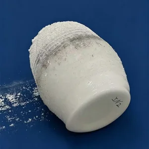
Pioneering High-Purity Fused Silica Engineering, Extreme Thermal Insulation Rings, and Plasma-Assisted Machining for Global Advanced Semiconductor, Photovoltaic, and Analytical Systems.
Engineered to exact micron tolerances, certified with 99.99% SiO₂ purity, and rigorously vacuum tested.




In modern semiconductor processing, etch chambers, and CVD/ALD diffusion reactors, the transparent quartz ring serves as a structural component, dielectric spacer, edge ring, and thermal insulator. Understanding its chemical and thermodynamic limits is essential for process yield optimization.
| Performance Parameter | Semiconductor Grade (Standard) | Advanced Optical/Plasma Grade | Functional Impact on Processing |
|---|---|---|---|
| Purity (SiO₂) | ≥ 99.99% (4N) | ≥ 99.999% (5N) | Prevents metallic ion contamination (Fe, Cu, Na) across wafer active zones. |
| Hydroxyl (OH⁻) Content | ≤ 20 - 30 ppm | ≤ 5 ppm (Low-OH synthetic option) | Controls IR transmission, high-temperature sag, and viscosity at >1100°C. |
| Thermal Shock Resistance | ΔT > 1000°C water quench | ΔT > 1100°C water quench | Withstands rapid thermal annealing (RTA) cycles without cracking. |
| Dielectric Strength | 25 - 40 kV/mm (at 20°C) | > 40 kV/mm (at 20°C) | Guarantees electrical insulation under high-frequency RF plasma bias. |
| Surface Roughness (Ra) | Ra ≤ 0.4 μm (Polished) | Ra ≤ 0.1 μm (Optical Fire-Polish) | Minimizes micro-particle generation in sub-7nm dry etching chambers. |
As the microelectronics and clean technology sectors advance, the demand for precision quartz rings shifts from generic glassblowing to nanoscale-controlled structural fabrication.
With transition toward 3D NAND (>200 layers) and Gate-All-Around (GAA) architectures, etch process recipes rely on corrosive halogen gases (CF₄, Cl₂, NF₃). Quartz rings must provide uniform plasma etch resistance, exceptional flatness, and zero micro-bubble inclusions to prevent wafer edge delamination.
High-efficiency N-type photovoltaic manufacturing lines utilize oversized LPCVD, PECVD, and POCl₃ diffusion systems. Rings operating in these high-throughput tubes must resist mechanical deformation under continuous 1100°C thermal loads while preserving vacuum seals against ambient air infiltration.
International procurement teams in North America, Europe, and Asia demand complete batch chemical assays (GDMS testing), CMM multi-axis dimensional validation, Class 100/1000 cleanroom packaging, and helium leak tightness guaranteed to less than 1.0×10⁻⁹ mbar·l/s.
Southeast Quartz operates a closed-loop fabrication ecosystem in Donghai, Jiangsu—the epicenter of global quartz processing—ensuring end-to-end quality control.
Utilizing high-purity natural silica sand processed through thermal arc plasma furnaces, producing bubble-free, stress-relieved cylindrical blanks ideal for custom quartz rings and flanges.
Advanced diamond-tooled CNC grinding and waterjet cutting ensure exacting concentricity, step chamfers, pinholes, and sealing O-ring grooves down to ±0.02 mm structural tolerances.
Oxy-hydrogen dynamic hot-working relieves microscopic surface micro-cracks generated during machining, creating an ultra-smooth, vitreous barrier against plasma erosion.
Computer-controlled electric annealing kilns eliminate internal birefringence stresses, followed by multi-stage ultra-pure HF/HNO₃ acid baths to strip surface metallic contaminations.
Engineered to satisfy the rigorous audit requirements of semiconductor foundries and research consortia worldwide.
Our manufacturing and processing units in Donghai adhere strictly to ISO 9001:2015 quality control principles, RoHS, and REACH international environmental safety regulations, ensuring free circulation across European and North American customs without restriction.
Every batch of quartz rings is accompanied by a Certificate of Analysis (CoA) containing Glow Discharge Mass Spectrometry (GDMS) readouts, confirming that critical contaminants such as Alkali Metals (Li, Na, K) and Transition Metals (Fe, Cu, Ni, Cr) are well below threshold limits.
Because fused quartz is vulnerable to micro-impacts during intercontinental transit, rings are vacuum-sealed in double-layer anti-static bags, suspended in custom high-density EPE foam cushions, and secured inside export-grade reinforced fumigation-free wooden crates.
Continuous investment in quartz processing research positions Southeast Quartz at the forefront of thermal and plasma component engineering.
Developing ultra-low OH synthetic fused silica rings using chemical vapor deposition (CVD-SiCl₄), achieving >99.9999% (6N) purity, virtually zero bubble count, and high deep-UV transmission for excimer laser and advanced photolithography tools.
Investigating plasma-sprayed yttrium oxide (Y₂O₃) and high-density anti-fluorine coatings on quartz ring perimeters to reduce etch rates in advanced CF₄/O₂ plasma environments by over 300%, extending replacement cycles.
Integrating CO₂ laser ablation for localized micro-stress correction and non-contact optical profilometry, establishing digital CAD-to-part verification with automated tolerance matching for Tier-1 equipment makers.
Everything you need to know when engineering and procuring custom transparent quartz rings.
Transparent fused quartz typically operates continuously at up to 1100°C and can sustain short-term exposures up to 1250°C. Its strain point is approximately 1075°C and softening point reaches 1683°C. To prevent devitrification (crystallization into cristobalite), avoid contamination from alkali metals (e.g., bare skin contact) before high-temperature heating.
Yes. We specialize in custom-engineered quartz components. Utilizing multi-axis CNC machines, laser cutters, and ultrasonic drilling systems, we machine intricate geometries, including alignment notches, gas distribution channels, ground bevels, step rings, and counterbore holes according to your technical drawings (CAD, DWG, DXF, or STEP format).
All vacuum-bearing and flanged quartzware undergoes helium mass spectrometry testing with a threshold sensitivity of <1.0×10⁻⁹ mbar·l/s. Furthermore, polariscope optical stress analyzers are utilized post-annealing to ensure that internal residual stress is minimized, preventing spontaneous failure during intense thermal transitions.
Standard prototypes and drawing reviews are processed in 24 hours. Small-batch prototyping usually takes 7 to 14 days, depending on tooling and raw material availability in our Donghai warehouse. High-volume continuous manufacturing runs typically take 3 to 4 weeks, inclusive of dimensional CMM inspection and cleanroom packaging.
Explore our complete manufacturing spectrum for high-heat, high-corrosion, and semiconductor environments.