Engineered to strict dimensional tolerances from optical-grade and semiconductor-certified fused silica. Helium mass spectrometry tested and verified for zero micro-fissures and ultra-trace metallic impurity levels.
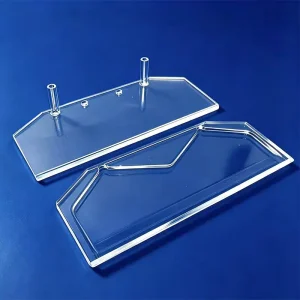





In high-density plasma etch, chemical vapor deposition (CVD), and advanced epitaxy reactors, quartz rings represent critical consumable hardware. Precise control over dielectric sheath physics, radial gas velocity, and thermal boundary layers demands strict structural engineering.
Engineered to sit concentric to 200mm, 300mm, and next-generation 450mm silicon wafers in capacitive coupled plasma (CCP) and inductive coupled plasma (ICP) etch chambers. By matching the dielectric impedance of the wafer surface, precision-machined quartz focus rings uniformize plasma sheath height right up to the outermost bevel, preventing wafer-edge critical dimension (CD) roll-off.
Widely deployed in atomic layer deposition (ALD), physical vapor deposition (PVD), and plasma-enhanced chemical vapor deposition (PECVD) reactors. These engineered rings physically shield mechanical electrostatic chuck (ESC) seals from reactive fluorine/chlorine chemistries and prevent parasite coating build-up on non-active wafer edge surfaces, mitigating particle flaking.
Utilized in rapid thermal processing (RTP) and horizontal/vertical quartz diffusion furnaces. Operating up to 1,200°C, these high-purity rings provide mechanical load bearing, thermal radiation buffering, and laminar gas partitioning, ensuring that precursor gases like SiH4, DCS, and POCl3 distribute with rotational symmetry across multi-wafer batch loads.
Sub-micron manufacturing processes cannot tolerate metallic contamination or structural devitrification. Southeast Quartz leverages both electro-fused natural quartz and synthetic vapor-phase CVD silica to match specific chamber etch rates and dielectric thresholds.
| Material Engineering Grade | SiO₂ Purity (%) | Hydroxyl (OH⁻) Content | Softening Point (°C) | Coefficient of Thermal Expansion (CTE) | Primary Industrial Sector |
|---|---|---|---|---|---|
| Semiconductor Electric Arc Fused (EQ-Grade) | ≥ 99.999% (5N) | < 5 – 30 ppm | ~ 1,683 °C | 5.5 × 10⁻⁷ / °C (20°C – 320°C) | Dry Plasma Etch / Diffusion |
| Synthetic Fused Silica (CVD / VAD Grade) | ≥ 99.9999% (6N-7N) | < 1 ppm (Dry) to 1,200 ppm | ~ 1,600 °C | 5.2 × 10⁻⁷ / °C | Sub-7nm Wafer Processing |
| Opaque Micro-Bubble Quartz (Solar Grade) | ≥ 99.99% (4N) | < 40 ppm | ~ 1,650 °C | 5.4 × 10⁻⁷ / °C | N-Type TOPCon / HJT Solar |
| Optical Grade HPFS (Homogeneity H4) | ≥ 99.9995% | Controlled 100–200 ppm | ~ 1,670 °C | 5.5 × 10⁻⁷ / °C | Excimer Laser Optical Ring Mounts |
Thermal stability is dictated by alkali metal concentrations (Na, K, Li). Total alkali impurities in our high-temperature quartz rings are systematically controlled below 0.8 ppm via specialized multi-stage chlorination and purification. This suppresses the nucleation of cristobalite crystalline phases even when running continuous 1,150°C furnace operations, eliminating premature micro-cracking and spalling during rapid cool-down cycles.
In high-frequency capacitive plasma systems (13.56 MHz to 60 MHz), non-uniform dielectric constants cause hot spots, localized RF arcing, and uneven etching depth. Our synthetic and plasma-fused raw quartz blocks undergo polarized interferometry and refractive index mapping to ensure spatial dielectric homogeneity (ε = 3.78 ± 0.02), ensuring uniform plasma densities and consistent RF coupling across the whole chamber circumference.
Southeast Quartz operates from Donghai County, Jiangsu — the world's most concentrated silicon and crystal processing hub. This geographic integration converts directly into cost leadership, raw material traceability, and rapid lead times for international semiconductor buyers.
Raw ultra-high-purity quartz sands (SiO2 > 99.999%), continuous electric melting, and plasma arc ingot fabrication are located within a 15km perimeter. This eliminates external logistics freight premiums and cuts raw stock procurement cycles from months to under 48 hours.
Equipped with 5-axis simultaneous ultrasonic grinding systems, high-speed diamond trepanning lathes, and computerized laser profilometers. We reliably deliver tight ring concentricity (±0.015mm), flatness (≤ 0.008mm), and Ra ≤ 0.2μm optical polished surface finishes.
Every machined quartz ring undergoes chemical acid etching (HF/HNO3 baths) to eliminate micro-cracks induced during cold grinding, followed by UPW (Ultra-Pure Water 18.2 MΩ·cm) ultrasonic cleaning and class 100 packaging for immediate wafer-fab chamber installation.
By eliminating multiple tiers of overseas brokers and trading entities, our direct factory-to-fab pricing offers a 35% to 55% Total Cost of Ownership (TCO) advantage over European, Japanese, or North American OEM spare component providers without sacrificing chamber lifetime.
Quartz rings undergo unique chemical, thermal, and mechanical stresses across different manufacturing sectors. Engineering geometry and material choice are tailored specifically to match operational chemistries.
In high-aspect-ratio (HAR) contact and trench etching chambers, high-energy fluorocarbon plasmas (CF4, C4F8, CHF3) strike the focus ring continuously. Our specialized dense-fused quartz rings minimize physical sputtering and uniformize plasma boundary potential, ensuring trench verticality and preventing tilt distortion across 128+ layer stacked memory arrays.
High-efficiency photovoltaic manufacturing utilizes oversized tubular Low-Pressure Chemical Vapor Deposition (LPCVD) and Plasma-Enhanced Chemical Vapor Deposition (PECVD) reactors. Large-diameter quartz isolation rings and carrier support rings isolate conductive poly-silicon layers, withstand continuous 850°C phosphorus oxychloride diffusion, and minimize micro-particle defects.
Optical rings and retaining collars constructed from high-transmittance fused silica serve as stable, stress-free mounting rings inside excimer laser lithography cavities, high-energy Nd:YAG resonators, and deep-UV spectroscopy cells. With low internal stress birefringence (≤ 5 nm/cm), our rings prevent beam wavefront distortion across high-intensity optical paths.
As critical dimensions compress below 2nm (GAA / RibbonFET architectures) and wafers scale to ultra-thin profiles, quartz ring engineering is evolving rapidly across three distinct technological axes.
Next-generation focus rings are increasingly combining fused quartz bases with atmospheric plasma-sprayed (APS) or atomic layer deposited (ALD) rare-earth oxide coatings (such as Y2O3, YOF, and YAG). This hybrid engineering achieves up to a 4× reduction in fluorine etch erosion rates, significantly extending consumable MTBC (Mean Time Between Cleans).
Uniform etch rates at the bevel require sophisticated aerodynamic stepped profiles on the ring face. Advanced CNC 5-axis ultrasonic multi-step machining can carve micro-grooves, gas relief channels, and sub-millimeter shoulders (±5μm tolerance) that balance fluid pressure and radical recombination rates directly over the bevel boundary.
Global semiconductor fabs are aggressively pursuing ESG initiatives. Heavily etched quartz rings are recovered, re-profiled via high-precision surface remachining, re-etched, fire-polished, and cleanroom-recertified. This recovers up to 70% of the quartz base value, drastically reducing embodied wafer-fab carbon footprints.
To ensure flawless first-pass qualification and eliminate costly design revisions, supply chain directors and chamber engineers must define clear dimensional, thermal, and surface requirements.
Every customized quartz ring manufactured at our facility is serialized and delivered with an exhaustive Quality Certification Dossier including:
Addressing critical engineering inquiries from process integration leads, equipment maintenance supervisors, and semiconductor procurement specialists.
Full catalog products engineered for extreme thermal shock environments, semiconductor diffusion furnaces, optical detection cells, and high-intensity industrial processing lines.

Send your CAD drawings (.DWG, .DXF, .STEP, or .PDF) directly to our senior quartz engineering team in Donghai, Jiangsu. We provide comprehensive manufacturability reviews, tolerance feedback, and factory-direct volume quotes within 24 hours.
