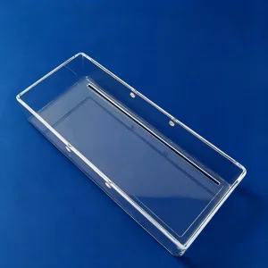
Explore our core baseline quartz hardware, engineered for high-temperature semiconductor furnaces, chemical reactor vessels, and optoelectronic enclosures with complete drawing customization.





A rigorous examination of synthetic versus naturally fused silica, internal transmission mechanics across deep UV through shortwave infrared, and critical structural thresholds for advanced optical instrumentation.
Technical Distinction: In precision optomechanics, the term "Fused Quartz" denotes amorphous silicon dioxide melted from refined natural quartz crystal, characterized by superior thermal creep resistance and high structural integrity at continuous 1,100 °C environments. Conversely, "Synthetic Fused Silica" is synthesized via chemical vapor deposition (gas-phase flame hydrolysis of silicon tetrachloride, SiCl₄, or organosilicon precursors). This chemical synthesis yields an isotropic, non-crystalline glass matrix essentially free of metallic trace elements (Fe, Al, Ti, Na < 0.1 ppm aggregate), delivering near-perfect optical homogeneity and transmission extending down to 185 nm in the Deep Ultraviolet (DUV) band.
Formed through flame hydrolysis of SiCl₄. Features an elevated hydroxyl content (-OH groups typically 800–1200 ppm), which eliminates absorption bands in the Deep Ultraviolet region while maintaining extreme optical transmission down to 185 nm.
Produced from electric or gas fusion of premium Donghai high-purity natural silica sand. Delivers exceptional transmission across 260 nm to 2600 nm, providing a cost-effective high-performance substrate for spectroscopy, sight glass viewports, and UV curing.
Treated through specialized vacuum induction desiccation to drive out -OH molecules (< 1 ppm residual hydroxyl). Completely cancels out the intense 2.73 µm absorption valley, ensuring flawless transmission spanning 250 nm up to 3500 nm in the mid-infrared.
| Property Parameter | JGS1 (Synthetic DUV) | JGS2 (Standard Optical) | JGS3 (Water-Free IR) | Testing Standard |
|---|---|---|---|---|
| Refractive Index ($n_d$ @ 587.6 nm) | 1.45846 ± 0.00005 | 1.45840 ± 0.00010 | 1.45842 ± 0.00005 | DIN 51423 / Abbe Metrology |
| Abbe Number ($V_d$) | 67.8 ± 0.5 | 67.8 ± 0.5 | 67.8 ± 0.5 | Calculated Optical Dispersion |
| Hydroxyl (-OH) Content | 800 – 1,200 ppm | 150 – 300 ppm | ≤ 1.0 ppm (Dry) | FTIR Infrared Spectroscopy |
| Coefficient of Thermal Expansion (CTE) | $5.5 \times 10^{-7}$ / K | $5.5 \times 10^{-7}$ / K | $5.4 \times 10^{-7}$ / K | Dilatometry (20°C to 320°C) |
| Laser Induced Damage Threshold (LIDT) | > 15.0 J/cm² (1064nm, 10ns, 20Hz) | > 6.5 J/cm² (1064nm, 10ns, 20Hz) | > 12.0 J/cm² (1064nm, 10ns, 20Hz) | ISO 21254-2 S-on-1 Protocol |
| Knoop Hardness (HK) | 522 kg/mm² | 522 kg/mm² | 522 kg/mm² | ASTM E384 Microindentation |
How Southeast Quartz leverages China's Silicon Valley of raw crystal processing to deliver uncompromising quality, accelerated turnaround times, and significant cost advantages to Tier-1 engineering firms worldwide.
Our foundry in Donghai County, Jiangsu, sits squarely at the core of the largest quartz processing trade corridor in Eurasia. This direct integration provides instant access to premium gas-fused and plasma-melted synthetic quartz ingots, eliminating raw stock lead times and supply disruption.
Unlike simple glass-cutting shops, our facility combines heavy-duty plasma-fusion workshops with high-precision 5-axis CNC diamond grinding, double-sided planetary planetary polishing (PR Hoffman systems), and laser-guided waterjet edging under an ISO Class 6 cleanroom enclosure.
Every custom optical window is qualified before packaging using helium mass-spectrometry leak detectors (< 1x10⁻⁹ mbar·L/s), Zygo Verifire GPI Fizeau interferometers for transmitted wavefront distortion, and PerkinElmer Lambda 1050+ spectrophotometers.
Market dynamics, technological catalysts, and material transitions accelerating adoption across next-generation semiconductor fabrication, high-power directed photonics, and quantum optomechanics.
With industrial fiber laser cutting heads breaching 30 kW to 60 kW power ratings, demand for anti-reflective coated fused silica protective windows with absorption levels below 5 ppm has skyrocketed to prevent thermal lensing and catastrophic blowout.
Advancements toward 3nm and 2nm semiconductor nodes necessitate optical inspection windows fabricated from ultra-pure synthetic silica with near-zero bubble density (DIN 58927 Class 0) and high resistance to 193 nm ArF excimer solarization.
As generative AI computing clusters migrate toward optical interconnects to overcome copper interconnect heat limits, micro-machined fused silica substrates with etched photonic wave pathways provide unrivaled thermal dissipation and zero signal phase drift.
Satellite observation optics require radiation-resistant cerium-doped or high-purity dry fused silica windows that sustain proton bombardment and cryogenic temperature cycling without darkening or wavefront distortion in Low Earth Orbit (LEO).
Fused silica optical flats engineered to perform where elevated temperatures, hazardous chemical reagents, high mechanical pressures, and intense laser fluences converge.
In molecular beam epitaxy (MBE), chemical vapor deposition (CVD), and particle beam accelerators, viewing ports must hold vacuum integrity below 10⁻¹⁰ Torr while transmitting analytical laser signals. Southeast Quartz provides fused silica discs hermetically brazed or Kovar-flanged (CF, ISO-K, KF formats) that undergo zero-leak mass-spectrometry certification.
From microfluidic DNA sequencing flowcells to industrial combustion gas analyzers, our synthetic silica optical windows provide flat baseline transmission across ultraviolet and near-infrared bands. Their non-fluorescent optical characteristics prevent signal distortion in critical fluorescence spectroscopy and medical diagnostics.
Equipped with dual-band or broadband anti-reflective (BBAR) multilayer dielectric coatings (reflectivity R < 0.2% at 1064 nm and 532 nm), our optical flats withstand high thermal gradients. They protect precision collimating and focusing optics from molten metal slag splatter and high-energy thermal radiation in industrial fabrication centers.
Fused silica displays chemical inertness against virtually all acids (except hydrofluoric and hot phosphoric acid) and withstands rapid thermal shock (e.g., dropping from 1,000 °C into room temperature water without microcracking). This resilience makes our windows ideal sight glass barriers for pilot plants and petrochemical reactors.
A comprehensive blueprint for optical engineers and international procurement leads specifying custom fused silica windows for industrial, scientific, and aerospace systems.
Specified per US Military standard MIL-PRF-13830B or ISO 10110-7. While commercial viewports often accept 60-40, precision high-energy laser and imaging systems require 20-10 or 10-5 scratch-dig to eliminate scattering centers and avoid localized laser ablation.
Measured using 632.8 nm He-Ne laser interferometers. Standard commercial options offer λ/2 to λ/4 per 25 mm diameter, while precision optical configurations achieve λ/10 to λ/20 P-V for diffraction-limited beam control.
Unless intentionally wedged (e.g., 30 arcmin to eliminate back-reflections in laser cavities), optical windows require parallelism tighter than 10 to 30 arcseconds (< 0.05 mrad beam deflection) across clear apertures.
In-depth insights addressing material selection, laser damage thresholds, environmental durability, and custom manufacturing parameters.
Complete product range covering high-temperature quartz lamp fixtures, engineered insulating glass rings, custom-slotted semiconductor wafer carriers, and process tubes.


Our senior optical engineering department confirms material manufacturability, laser damage limits, coating curves, and firm production lead times within 24 hours of technical file receipt.
Submit your PDF, DWG, DXF, or 3D STEP engineering drawings along with required substrate grade (JGS1, JGS2, JGS3), dimensional tolerances, surface quality (MIL scratch-dig or ISO 10110), and operational laser wavelength.
