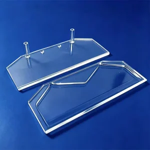
Explore our foundational range of precision quartz digestion tubes, custom machined fused silica plates, oversized furnace tubes, and insulation components engineered for extreme thermal and high-vacuum processing environments.
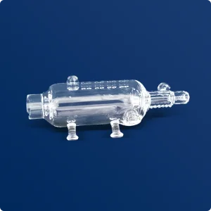




A rigorous examination of surface micro-roughness engineering, devitrification mitigation, and chemical-thermal dynamics across sub-10nm microelectronics fabrication lines.
In modern high-precision microelectronics, photovoltaic cell fabrication, and thin-film epitaxy, substrate holders must overcome intense mechanical stresses, extreme thermal shock, and aggressive chemical degradation. While optical-grade, transparent fused silica has historically dominated process chambers, frosted quartz substrate holders have emerged as an indispensable engineering solution. By intentionally introducing a precision-controlled micro-textured topography—achieved via computerized micro-sandblasting or hydrofluoric chemical etching—frosted quartz holders resolve severe industrial challenges including thermal radiation hotspotting, vacuum-stiction adhesion, substrate slippage, and stray optical interference.
Understanding the operational thresholds of fused silica substrate holders requires deep comprehension of raw ingot selection, network hydroxyl ([OH⁻]) concentration, and crystallization thermodynamics. Lianyungang Southeast Quartz sources raw crystal aggregates exclusively from Donghai's world-renowned quartz formation zone, utilizing specialized flame fusing and electric fusion processes that ensure zero bubble inclusions (DIN 58927 Class 0/1) and an exceptionally low thermal expansion coefficient.
| Physical / Chemical Property | Standard Clear Quartz | Frosted Quartz (Southeast Quartz Grade) | Operational Impact on Substrates |
|---|---|---|---|
| Silica Purity (SiO₂) | 99.99% | ≥ 99.995% to 99.999% | Prevents trace transition metal migration (Fe, Cu, Ni) into wafer junctions. |
| Surface Roughness (Ra) | Ra < 0.02 µm (Polished) | Ra 0.8 µm to 6.5 µm (Custom) | Prevents wafer sticking via vacuum-lock; optimizes friction coefficient. |
| Thermal Expansion (CTE) | 5.5 × 10⁻⁷ / K (20–320°C) | 5.4 – 5.6 × 10⁻⁷ / K | Virtually zero dimensional distortion under rapid 200°C/min temperature ramping. |
| Softening Point | 1,683°C | 1,685°C – 1,710°C (Annealed) | Resists creep deformation during high-load horizontal furnace insertion. |
| Annealing Point | 1,215°C | 1,220°C | Relieves structural micro-stresses created during precision CNC machining. |
| Total Hydroxyl ([OH⁻]) Content | < 30 ppm (Flame Fused) | < 5 – 15 ppm (Dehydroxylated) | Suppresses thermal sagging and structural swelling under long-cycle high-temp vacuum. |
Engineered to satisfy demanding operational protocols across semiconductor fabs, photovoltaic cell lines, optical metrology suites, and hazardous chemical research installations.
Frosted quartz substrate holders are universally deployed in wet chemical processing benches, serving as acid-resistant wafer chucks, lifter pins, and cassette carriers.
Critical in high-throughput N-type TOPCon POCl₃ diffusion and LPCVD passivated contact deposition furnaces operating at 800°C–1,050°C continuously.
Used as planetary carrier plates, shadow mask frames, and lift stages inside high-vacuum electron-beam evaporation and magnetron sputtering tools.
Non-reflective matte quartz backplates used in optical inspection tables, UV laser ablation chambers, and glass microfluidic biochip alignment jigs.
Anticipating the structural, thermodynamic, and dimensional challenges of future 2nm logic nodes, 3D NAND scaling, and ultra-large panel-level packaging architectures.
Traditional random sandblasting produces micro-notches that act as fracture origination points. Southeast Quartz is pioneering multi-axis slurry blasting combined with controlled chemical acid smoothing.
This closed-loop surface metrology yields a tightly controlled Ra profile (e.g., exactly Ra 1.8 ± 0.2 µm) with plateau-like peaks. The resulting surface eliminates particulate shedding during robotic transfers while drastically improving wafer thermal contact stability.
As reactive ion etching (RIE) transitions toward denser fluorine-based plasmas (NF₃, CF₄, SF₆), quartz tooling suffers accelerated sputtering erosion and silicon oxyfluoride grain erosion.
Our R&D roadmap integrates surface densification via thermal plasma glazing and atomic layer deposited (ALD) yttria/alumina barrier phases directly on frosted quartz surfaces. This innovation extends substrate holder lifespan in hostile plasma chambers by over 300% without introducing metallic contaminants.
Advanced packaging is transitioning from 300mm round wafers to 510×515mm and 600×600mm rectangular glass and synthetic panels to maximize semiconductor packaging density.
We have commissioned oversized 5-axis CNC diamond grinding and ultrasonic milling centers capable of producing monolithic frosted quartz substrate carrier trays up to 1,200 mm in lateral dimensions, maintaining an overall flatness tolerance under 15 microns across the entire active surface.
How vertical integration, raw material localization, and mature glasswork craftsmanship create an unrivaled cost-to-performance ratio and resilient delivery pipelines.
Situated in Donghai County, Jiangsu—the premier quartz resource and manufacturing capital of the Eurasian continent—Southeast Quartz operates directly at the primary source of global high-purity natural silica.
Immediate access to premium silica sands, plasma-fused quartz ingots, and oversized mother tubes shields our international procurement partners from supply shortages and catastrophic logistics markups that cripple fragmented assemblers.
While European and North American quartz workshops quote 12 to 18 weeks for non-standard tooling, our integrated workshop completes custom drawing reviews within 24 hours and delivers verified prototypes in 10 to 14 days.
With multi-axis CNC cold-cutting, flame lathe hot-working, and cleanroom acid leaching coordinated under a single factory roof, we drastically compress development cycles for Tier-1 equipment makers.
Leveraging high-yield automated cutting lines and proprietary tooling fixtures (backed by over 200 utility model patents), we deliver premium-grade fused quartzware at 30% to 50% below historical Western OEM pricing.
Our expansive production footprint maintains redundant furnace capacity and a minimum 6-month buffer of certified quartz ingot stock, insulating clients from raw commodity fluctuations.
Strategic insights into wafer fab capacity expansions, dual-sourcing procurement trends, and the critical importance of vendor qualification in volatile geopolitics.
The global semiconductor and clean energy landscape is experiencing unprecedented geographical decentralization. As multi-billion-dollar wafer fabs, solar gigafactories, and advanced packaging plants expand across North America, Europe, Japan, and Southeast Asia, consumable quartzware has emerged as a major operational bottleneck. Quartz components—including substrate holders, furnace tubes, and transfer boats—are not one-time capital expenditures; they are wear items subjected to cyclical etching, aggressive chemical cleanings, and thermal fatigue, necessitating scheduled replacement every 3 to 18 months.
Historically, global chipmakers relied almost exclusively on single-source Japanese or German quartz suppliers. However, prolonged lead times exceeding 50 weeks during recent supply shocks forced procurement directors to systematically re-evaluate their supply chains. Modern wafer fabs now aggressively pursue dual-sourcing strategies, validating high-capability Chinese manufacturers who can meet or exceed SEMI dimensional standards, helium leak tightness, and sub-ppb impurity thresholds.
Our export compliance protocol provides comprehensive traceability from raw mineral lot numbers through cleanroom packaging, guaranteeing clear supply chain audits for multinational compliance.
By extending component operational life through optimized micro-frosting and stress-free annealing, fab operators reduce unscheduled furnace downtime and lower annual consumables spend.
We work directly from customer CAD drawings (STEP, DWG, PDF) or reverse-engineer legacy components with micron-accurate 3D laser scanners to support older fab line maintenance.
Zero-defect manufacturing supported by advanced physical verification, helium mass spectrometry, and comprehensive material traceability.
Every welded joint, flanged fitting, and sealed chamber undergoes helium mass spectrometry testing down to leak rates < 1×10⁻⁹ mbar·l/s, ensuring vacuum integrity.
High-precision non-contact vision CMM systems verify complex slot profiles, pitch tolerances (±0.02 mm), and overall flatness on holders up to 1,500 mm.
Inductively Coupled Plasma Mass Spectrometry monitors 24 trace metal elements (Al, Fe, Cu, Ti, Na, K, Li), maintaining total metal impurities below 15 ppm.
Multi-stage ultrasonic bath cleaning with electronic-grade high-purity HF/HNO₃ acids, 18.2 MΩ·cm DI water cascade rinsing, and Class 100 double-layer vacuum packaging.
Essential guidance addressing material selection, frosting specifications, devitrification thresholds, and custom prototyping protocols.
Explore heat-resistant quartz lamp holders, oversized process tubes, optical plates, and microchannel devices built to exact customer drawings and specifications.