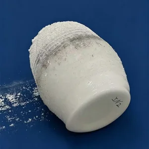
Direct-from-factory high-temperature insulation rings, oversized furnace chambers, slotted quartz carriers, and custom lab-scale thermal platforms manufactured under ISO9001 certified protocols.

An in-depth analysis of raw material refinement, thermal kinetics, crystallization prevention, and the physics governing amorphous silicon dioxide performance.
The core threshold of semiconductor-grade melting quartz rests upon minimizing non-silicon trace elements. Metallic impurities such as Fe, Al, Ti, alongside alkali ions like Li, Na, and K, act as nucleation catalysts. Our purification process combines advanced thermal chlorination with multi-stage chemical leaching to ensure total metallic contaminants stay strictly below 15-20 ppm, ensuring absolute chemical inertness during wafer processing.
Fused silica features a virtually zero thermal expansion coefficient (5.5 × 10⁻⁷/K), granting supreme shock immunity up to thermal peaks of 1250°C. However, prolonged operation above 1100°C in the presence of surface moisture or alkalis accelerates phase transition from the vitreous state into cristobalite. Advanced electro-fusion protocols suppress structural hydroxyl (OH-) concentration to preserve high-load structural elasticity.
By employing high-frequency induction plasma torches running under vacuum conditions, natural high-purity crystalline quartz sands undergo spontaneous phase transition without graphite crucible contamination. The resulting vitreous ingots feature near-zero microscopic bubble fractions, zero striae, and isotropic optical transmission across deep ultraviolet (DUV) through mid-range infrared spectra.
Understanding how the integration of raw material clusters in Donghai, high-temperature flame hot working, and advanced cold CNC centers provide unrivaled capital efficiency.
Situated in Donghai County—the globally recognized epicenter of quartz refining—our facilities have instantaneous, bulk-scale access to top-tier quartz sand and feedstock. This vertical proximity eliminates long-distance transit oxidation risks, reduces internal shipping lead times to hours, and locks in raw material cost stability despite global market fluctuations.
Modern melting quartz demands both classical hot-fire bench craftsmanship and multi-axis automated CNC diamond routing. Our factory floor operates dynamic glassblowing lathes capable of handling oversized diameters up to 600mm+, paired with ultrasonic milling machines to achieve dimensional tolerances within ±0.05mm on custom flanges, slots, and optical planar windows.
Eliminating contamination points before high-value deployment is paramount. In-house helium mass spectrometer leak detectors certify pressure vessels, while laser interferometers assess surface flatness. Every custom order undergoes hot-annealing cycles inside automated kilns to release internal residual shear stresses, effectively avoiding catastrophic runtime fracturing.
How next-generation semiconductor nodes, TOPCon/Heterojunction solar cells, and ultraviolet water processing are transforming raw melting quartz specs.
The global shift toward high-efficiency solar cells demands large-diameter horizontal and vertical furnace tubes. In low-pressure chemical vapor deposition (LPCVD) and boron/phosphorus diffusion, melting quartz tubes must endure intense corrosive dopants (POCl₃, BBr₃) at elevated temperatures without thermal warping, ensuring optimal wafer yield and longer replacement intervals.
As semiconductor lithography advances into sub-nanometer regimes, etch chamber rings, showerheads, and bell jars must withstand aggressive fluorinated and chlorinated plasma environments. Plasma-fused quartz guarantees ultra-high density and an exceptionally low micro-void index, preventing particle flaking that compromises microchip yield rates.
Water treatment facilities and high-speed coating lines utilize specialized UV discharge lamps. Melting quartz glass tubes serve as the premier protective casing due to their exceptional transmission across the germicidal UVC spectrum (254nm). Their thermal shock resilience allows flash cooling under pressurized fluid currents without mechanical fracturing.
Laboratory spectrometry, continuous flow-cell analysis, and laser optics require high optical transmission from UV to near-infrared wavelengths. Precision-polished fused quartz plates and custom-machined microchannels eliminate background optical scatter and fluorescence, providing analytical laboratories with baseline measurement stability.
Streamlined protocols designed to simplify drawing-based procurement, supply line visibility, batch consistency, and ocean freight security for overseas buyers.
Procurement teams require direct engineering accountability. Our technical group reviews DWG, DXF, or 3D STEP models within 24 hours to verify hot-working radii, structural tolerance allowances, and tooling feasibility before initial fabrication begins, eliminating expensive downstream tooling modifications.
Every fabrication run is logged against its corresponding batch of fused quartz ingot or tubular parent stock. Standard documentation includes ICP-MS trace element breakdown, surface roughness (Ra) records, and optical transmission certifications to verify international compliance.
Mitigating in-transit mechanical shock is critical when exporting brittle materials. Our components use multi-density PE contoured cutouts, vacuum-sealed electrostatic wrapping, and ISPM-15 compliant export timber crates, maintaining an intact delivery record above 99.8% across global logistics channels.
Comprehensive engineering and procurement answers covering melting quartz performance, custom tolerances, failure modes, and supply logistics.
Explore our complete catalog of industrial fused silica items, plasma-fused ingots, optical-grade substrates, and precision wafer processing accessories.