Engineered to tight dimensional tolerances with extreme thermal stability, chemical inertness, and ultra-high chemical purity exceeding 99.99% SiO₂.




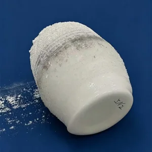


Strategic overview of global quartz market dynamics across tier-1 semiconductor fabrication, advanced optical communication, and extreme industrial environments.
Within sub-7nm node semiconductor manufacturing, standard borosilicate or float glass cannot withstand plasma etching, dry oxidation, or wet chemical baths. Fused quartz slides and substrates deliver zero thermal distortion under intense UV exposure and exceptional resistance to hydrofluoric acid gas vapor.
Biomedical platforms rely on synthetic fused silica microscope slides to achieve broad spectral transmission extending deeply into deep-ultraviolet (DUV, down to 190 nm) and near-infrared spectra without the background autofluorescence typical of soda-lime alternatives.
Photovoltaic wafer processing demands giant thermal quartz carriers and slide boats capable of cycling repeatedly from 600°C to 1150°C during boron/phosphorus diffusion without warping, flaking, or introducing transitional metal contamination into crystalline structures.
Comprehensive transition roadmap from natural quartz fusion toward synthetic laser-grade silica architectures with atomic-level surface flatness.
Electric-arc vacuum thermal fusion and chemical vapor deposition reducing iron, copper, and alkali ions below 0.1 ppm to prevent devitrification and electrical cross-talk.
High-speed diamond grinding, ultrasonic hole drilling, laser dicing, and multi-axis edge beveling to prevent mechanical edge chipping and micro-cracking.
Chemical Mechanical Planarization (CMP) delivering surface roughness Ra < 0.5 nm, flatness λ/4 to λ/10 per inch, and scratch-dig standards of 20/10.
Total vacuum helium leak testing (< 1×10⁻⁹ mbar·L/s), FTIR spectrometry testing, and optical polariscope strain inspections before Class 100 clean packaging.
Turnkey fused silica engineering serving international cleanrooms, research institutes, and original equipment manufacturers.
From one-off laboratory slide prototypes to automated multi-thousand wafer run containers. Full compatibility with STEP, DWG, and PDF technical drawings with turnaround engineering reviews completed within 24 hours.
Ultra-pure multi-stage acid pickling (HF/HNO₃ balance) accompanied by 18.2 MΩ·cm deionized water ultrasound purging ensures surfaces are completely free of organic particles, sodium, and heavy metal residues.
Automated programmed electric annealing up to 1215°C with slow-cooling thermal ramps guarantees zero internal birefringence, eliminating sudden thermal cracking during intensive rapid thermal processing (RTP).
Factory-direct fused silica slides, furnace tubes, custom insulation components, and high-performance quartz glassware.

Critical engineering considerations, material purity grades, and manufacturing thresholds answered directly by our factory technical directors.
