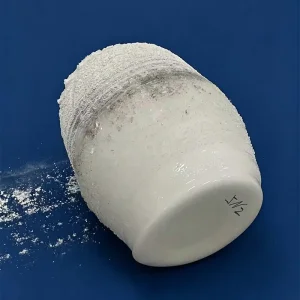
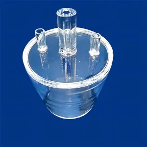
Explore our foundational range of direct-factory quartz tooling, furnace apparatus, and specialized high-temperature carriers verified for zero thermal distortion.



In modern microfabrication, horizontal and vertical quartz tray boats act as critical wafer-holding infrastructure within LPCVD, thermal oxidation, and plasma diffusion environments.
Continuous cycling across semiconductor thermal budgets demands ultra-low coefficients of thermal expansion (5.5 × 10⁻⁷/°C). Our fused silica boats resist softening, sagging, and structural warping through multi-stage anneal regimens.
Trace metal contamination (Fe, Cu, Ni, Na, K) can degrade wafer carrier lifetime and cause junction leakage. Our Donghai natural and synthetic plasma-fused raw materials ensure zero volatile contaminant outgassing inside cleanrooms.
Wafer pitch uniformity is paramount for consistent laminar gas flow. Equipped with 5-axis CNC diamond grinding heads, we fabricate slots with angular accuracy under ±0.05 mm to prevent edge chipping or micro-scratching on fragile substrates.
Positioned inside China's primary silica processing hub in Donghai County, Jiangsu, Lianyungang Southeast Quartz leverages an end-to-end manufacturing footprint that dramatically reduces global lead times.
Immediate access to domestic crystalline silica resources and electric-arc/plasma melting capabilities reduces raw material transport costs and delivers uncompromised traceability from quartz ingot to finished boat.
Standard carrier prototypes are completed in as few as 7 working days. In-house flame hot-working and CNC ultrasonic grinding lines remove multi-vendor subcontracting bottlenecks.
Continuous batch processing and semi-automated laser dimensional inspection yield significant component cost reductions over European and North American regional distributors without sacrificing SEMI standards.
Quartz boats undergo rigorous stress evaluation across four major global industrial process categories.
Applied in horizontal tube furnaces for Boron and Phosphorus pre-deposition and drive-in diffusion at operating profiles reaching 1,000°C to 1,150°C under N₂, O₂, or forming gas chemistry.
Accommodates oversized thin M10, G12, and rectangular silicon wafers during low-pressure chemical vapor deposition (LPCVD) and PECVD poly-Si layer growth with anti-stick surface profiles.
Supports sapphire, GaAs, and SiC wafers inside epitaxial batch processing and MOCVD chambers where chemical inertness against harsh fluoride cleanings is strictly demanded.
Serves as contamination-free combustion boats and sintering trays within university, metallurgical, and battery cathode analysis laboratories requiring unreactive thermal containment.
Understand why fused quartz remains the gold standard compared to alumina and silicon carbide across wafer-level thermal operations.
| Performance Characteristic | High-Purity Fused Quartz | High-Alumina Ceramics (99% Al₂O₃) | Recrystallized SiC |
|---|---|---|---|
| Thermal Shock Resistance | Exceptional (Quench from 1,000°C without crack) | Moderate (Susceptible to rapid gradient spalling) | Good (High thermal conductivity helps disperse shock) |
| Purity & Outgassing (ppm) | < 15 ppm total metallic impurities | > 500 ppm trace alkali/transitional metals | Requires expensive CVD coatings to prevent metal drift |
| Acid Slurry Resistance (HF/HNO₃) | Moderate attack by HF; insoluble in most mineral acids | Poor in concentrated mineral acid cleans | Excellent chemical endurance across acids |
| Component Cost & Replacement | High cost-efficiency, rapid customized rework | High tooling and die cost; brittle handling | Very high initial capex (4x to 8x higher than quartz) |
As semiconductor wafer node transitions accelerate and solar wafer formats expand to 210mm+, the technical specifications for quartz tray boats continue to elevate.
For sub-14nm semiconductor wafer lines, standard electric-fused quartz is increasingly complemented by synthetic quartz materials that deliver single-digit ppb metal counts and minimize OH radical content.
Modern fab robotic transfer arms (EFEM) require tighter outer dimensional tolerances (±0.03 mm) and reinforced quartz structural rails to prevent displacement during 300mm wafer transfer cycles.
Procurement directors seek suppliers offering etched 2D matrix serial numbers, laser batch certificates, and structured wafer carrier rework programs to lower total cost of ownership (TCO).
Authoritative answers covering mechanical tolerances, devitrification mitigation, and custom CAD specifications.
Devitrification occurs when trace alkaline ions (Na, K, Ca) act as crystallization nuclei above 1,000°C. We conduct ultra-pure 18MΩ deionized water flushing and multi-stage 10% HF acid etch passivation in ISO cleanrooms before shipment. Operators must maintain strict particulate-free handling using nitrile gloves and acid-clean boats after process runs.
Using diamond-tipped computerized slicing and multi-blade CNC dicing, our typical tolerance for slot pitch is ±0.05 mm, with slot width tolerances held within ±0.03 mm. We can accommodate custom asymmetrical pitch spacings designed for automated robotic pick-and-place systems without localized micro-cracking.
Yes. Our in-house engineering group evaluates CAD files in STEP, IGES, DXF, or PDF format. We review structural load balancing, stress concentration radii at flame-welded joints, and thermal gas dynamic flow paths before providing a comprehensive DFM (Design for Manufacturability) proposal within 24 hours.
Every shipment is accompanied by a Certificate of Analysis (CoA) documenting ICP-MS trace metal impurity limits, coordinate measuring machine (CMM) dimensional inspection reports, and polariscope optical stress evaluation reports verifying full internal stress-relief annealing.
Continuous-draw tubes, plasma-fused quartz ingots, and chemical precursor bubblers built to support demanding fab uptime.