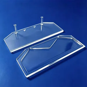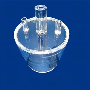
Engineering high-purity (≥99.99% SiO₂) fused quartz components, wafer diffusion boats, furnace tubes, and fluid accessories. Built to SEMI standards with sub-micron precision for international cleanrooms and next-generation fabs.
Essential process-grade thermal tooling, chemical vapor vessels, and ultra-high purity vacuum tubes direct from our Donghai facility.





Advanced node scaling (sub-5nm), compound semiconductor ramp-ups (SiC/GaN), and 3D NAND fabrication requirements.
The semiconductor wafer fabrication landscape is undergoing a structural paradigm shift. As lithography approaches physical quantum limits and architectures transition from FinFET to Gate-All-Around (GAA) nanosheets, contamination tolerances have narrowed to parts-per-billion (ppb) and parts-per-trillion (ppt) regimes. In thermal processing chambers—encompassing atmospheric oxidation, LPCVD, atomic layer deposition (ALD), and high-temperature drive-in diffusion—quartz wafer processing accessories operate at the thermal and mechanical core of operational yield.
A single atomic PPM contamination of alkali elements such as Sodium (Na), Potassium (K), or heavy metals like Iron (Fe) and Copper (Cu) can trigger dielectric breakdown, threshold voltage drift, or lifetime degradation in active channels. Modern wholesale procurement has consequently moved beyond standard commercial silica. Sourcing directors and fab integration teams now mandate synthetically plasma-fused or electro-thermally refined synthetic ingots, coupled with micro-structural controls that minimize bubble count, eliminate particulate seed nucleation, and guarantee continuous heat resistance past 1,150°C.
Larger diameter wafers incur severe slip dislocation risks across vertical furnace cycles. Contemporary quartz boats and cantilever paddles feature finite-element-optimized slot geometries that mitigate edge stress and maximize radial heat symmetry.
Chlorine, fluorine, and bromine-based plasma etching chemistry severely corrodes conventional vitreous silica. Advanced synthetic quartz glass accessories feature zero internal porosity, suppressing chemical etching rates and micro-flaking.
Silicon Carbide epitaxy and annealing push operational temperatures past 1,600°C. While standard quartz reaches its softening point near 1,683°C, specialized thermal shields, opaque fused silica baffles, and cold-machined quartz rings safeguard process chambers.
How Tier-1 foundries, OSAT facilities, and equipment OEMs qualify wholesale quartz manufacturing partners.
Global procurement divisions evaluate suppliers through stringent audits covering material provenance, processing capability, metrology consistency, and total cost of ownership (TCO). In semiconductor diffusion operations, equipment downtime directly scales with furnace accessory longevity. Replacing a quartz tube or carrier boat costs far more in lost chamber qualification time than the component's capital expense. As such, procurement managers apply strict E-E-A-T criteria:
Automated wafer transfer robots (WTR) require pitch tolerances within ±0.05mm. Slot skew or thermal sagging in quartz wafer boats disrupts vacuum chuck engagement, risking catastrophic multi-wafer drops inside sealed furnaces.
Every wholesale batch must be accompanied by GDMS (Glow Discharge Mass Spectrometry) or ICP-MS analytical reports confirming trace metal levels remain strictly under 0.1 ppm across critical metallic elements.
Process chambers handling silane (SiH₄), arsine (AsH₃), or dichlorosilane (DCS) demand zero helium leakage. Welded joints, flanges, and bubbler connection ports must verify helium leak rates below 1×10⁻⁹ mbar·L/s.
Combining Donghai’s raw silica reserves with multi-axis CNC robotics, cleanroom purification, and localized vertical integration.
Situated in Donghai County, Jiangsu—the premier raw and refined quartz ecosystem on the Eurasian continent—Southeast Quartz bridges geological raw material supremacy with Industry 4.0 precision engineering. The historical bottleneck in quartzware fabrication has been excessive dependence on manual glassblowing, which introduces human variability in wall thickness, slot symmetry, and structural residual stress.
Our manufacturing facility utilizes a hybrid production matrix. Raw quartz sand undergoes proprietary multi-stage flotation, magnetic separation, and plasma gas refining to minimize internal bubbles and hydroxyl (OH-) content. CNC multi-axis ultrasonic milling machines, automated glass lathes, and laser profile trackers conduct cold slotting and hot welding under continuous algorithmic oversight. Each component passes through computerized de-stressing annealing lehrs, followed by hydrofluoric-nitric ultrasonic cleaning and Class 100/1000 cleanroom vacuum packaging. This integrated ecosystem protects global supply chains from lead-time volatility while maintaining strict repeatability.
Engineered to perform in the semiconductor, photovoltaic, analytical, and optoelectronic domains.
Quartz boats, horizontal cantilever systems, and diffusion tubes sustain continuous 1,000°C to 1,200°C thermal cycles during boron and phosphorus doping, drive-in oxidation, and high-k gate dielectric preparation.
Oversized quartz tubes with diameters exceeding 400mm-600mm house high-throughput batch solar wafers during POCl₃ diffusion and LPCVD poly-silicon deposition, preventing slip lines and maximizing conversion efficiency.
3-port bubblers, source jars, and wet oxidation bottles manage hazardous chemical transport (TEOS, POCl₃, BBr₃), delivering stable carrier gas saturation without chemical degradation or particulate generation.
High-purity quartz focus rings and chamber wall shields shield metal reactor chambers from aggressive fluorinated (CF₄, SF₆) reactive ion etching, eliminating metal back-sputtering onto patterned wafers.
Precision-annealed quartz bell jars maintain structural integrity under high vacuum (<10⁻⁶ Torr) and rapid thermal cycling during electron-beam physical vapor deposition (E-beam PVD) and optical thin-film coating.
Micro-machined quartz chips and spectrophotometer optical windows facilitate high-accuracy fluorescence microscopy, HPLC spectrometry, and deep-UV laser inspection across semiconductor metrology.
Technical guidance on chemical composition, manufacturing tolerances, devitrification, and custom production.
Precision-machined rods, flow cells, oversized tubes, and bespoke semiconductor glass instruments.