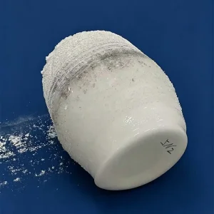
Engineered for low particle generation, zero ionic cross-contamination, and extreme thermal resilience across sub-micron diffusion lines.
Demanding semiconductor fabricators, national laboratories, and advanced thermal-process fabs in the United States require verifiable glass purity, tight radial tolerances, and zero trace-metal leaching.
Trace metal contaminants like Fe, Cu, Ni, Na, Li act as deep-level recombination centers in silicon crystal lattices. Our raw silica feedstocks undergo dynamic plasma purifying to preserve carrier lifetimes during CVD and dry oxidation phases.
With an extremely low linear expansion coefficient of 5.5 × 10⁻⁷/K, our furnace tubes survive acute thermal ramping between 20°C and 1,150°C without mechanical micro-fracturing or wall bowing during horizontal wafer boat cycles.
High-vacuum and hazardous precursor applications demand absolute seal containment. Every finished flanged tube undergoes helium sniffer leak detection with rejection thresholds calibrated to < 1×10⁻⁹ mbar·l/s.
| Property / Characteristic | Standard Optical/Commercial Grade | Southeast Semiconductor Grade (SE-Ultra) | Test Standard / Evaluation Methodology |
|---|---|---|---|
| Silicon Dioxide (SiO₂) Content | 99.9% | ≥ 99.995% to 99.999% | Inductively Coupled Plasma Mass Spectrometry (ICP-MS) |
| Hydroxyl (OH⁻) Content | 150 – 200 ppm | < 5 ppm to < 20 ppm (Custom Annealed) | FTIR Infrared Absorption Spectrometry |
| Annealing Point | 1,120 °C | 1,215 °C | ASTM C598 Beam Bending Viscometry |
| Deformation / Softening Point | 1,630 °C | 1,683 °C | Dilatometric Softening Characterization |
| Thermal Shock Resistance | 1,000 °C to 20 °C Water Quench | 1,150 °C to Cold Water (No Failure) | Thermal Shock Cyclic Rapid Ingress Testing |
Addressing the stringent engineering risk frameworks and cross-border trade compliances required by American OEMs and Tier-1 fab operators.
Every drawing received in Imperial (inch) or Metric units is translated into tight dimensional control schemas adhering to SEMI E1.1 specifications. We support customer-specified ASME flange alignments, custom ground taper joints, and O-ring groove geometries.
We eliminate supply friction by managing complete US customs compliance under HTS Code 7002.31.00 (Tubes of fused quartz or other fused silica). We manage Section 301 filings, cargo clearance, and insured door-to-door transit to cleanrooms in California, Texas, Oregon, and Arizona.
Full batch provenance records are paired with every shipment. Customers receive certificates of analysis (COA) specifying trace metals down to parts-per-billion (ppb), confirming strict adherence to EU RoHS Directive 2011/65/EU and US TSCA Section 6 guidelines.
Direct integration with the world’s most concentrated quartz refining cluster delivers unmatched economies of scale, prototype velocity, and raw material access.
Situated in Donghai County, Jiangsu Province—the premier silica processing capital—we secure first-line allocations of ultra-pure crystal feedstocks and large-bore cylinder precursors. This raw-material hub architecture insulates our global clients from supply bottlenecks and reduces custom ingot turnaround times by over 40% compared to fragmented western fabricators.
Our workshop pairs 5-axis ultrasonic CNC diamond machining with hydrogen-oxygen thermal glass-blowing lathes capable of swinging diameters up to 650mm OD. From precision laser-slotted wafer boats to flanged furnace tube weldments, all operations take place within standardized clean environments to prevent ambient micro-particulate embedding.
How specialized quartz furnace assemblies perform across semiconductor fabrication, photovoltaics, aerospace, and synthesis laboratories.
Supporting low-pressure chemical vapor deposition lines depositing silicon nitride (Si₃N₄) and polysilicon where absolute airtightness at 800°C–1,000°C prevents atmospheric back-streaming and pinhole defects.
High-resistivity silicon wafer diffusion requiring thick-walled quartz process tubes resistant to corrosive dry Cl₂ or wet steam atmospheres at operating temperatures up to 1,150°C without devitrifying.
Large-diameter oversized tubes (OD > 350mm to 550mm) serving next-generation solar cell manufacturing, maintaining bore straightness over lengths exceeding 2,500mm.
Thermal shielding, sight windows, and high-temp vacuum combustion tubes used in university research reactors, defense prototyping, and laser ignition research chambers across North America.
Analyzing key shifts impacting semiconductor equipment supply chains over the next five years.
As wafer sizes stabilize at 300mm and transition toward 450mm test cells, furnace tube camber (total indicator runout, TIR) specifications have tightened from ±1.0mm/m down to ≤ 0.3mm/m to guarantee smooth robotic loading without wafer cassette clipping.
High-thermal recipes running past 1,100°C trigger viscous flow in quartz with elevated OH concentrations. Low-hydroxyl synthesis (<10 ppm OH) significantly elevates the softening point, extending structural service lifetimes before replacement.
Procurement directors increasingly bypass intermediate glass trading entities. By collaborating directly with primary fabricators possessing both cold CNC and hot flame capacity, engineering revisions clear in hours instead of weeks, reducing unit acquisition costs by 25–40%.
Essential guidance on specifying parameters, preventing thermal devitrification, and arranging insured maritime and air shipping.
Explore customized rings, high-durability plates, source holders, and plasma-melted components engineered to tight print tolerances.